- Relays & Contactors
- Semiconductor Relays
PhotoMOS® FAQs
Table of contents
- How to shorten the operate/release time of PhotoMOS® relays?
- Are PhotoMOS® suitable for Reed Relay Replacement?
- The peak load current in the rating table is based on 100-ms application (1 shot). Can a higher current be applied if the time is shorter?
- How should I choose an input-limiting resistor for PhotoMOS® (assuming constant voltage source)?
- A diode is placed in parallel with the output MOSFET. Can it be used as a clamp diode?
- The catalog does not include the minimum applicable load value. What is the lowest current that can be correctly controlled by PhotoMOS®?
- Is it possible to increase the load current value of PhotoMOS® by decreasing the load voltage from the specified absolute maximum rating?
- What are the differences among the typical and maximum LED operation currents, and the LED input current?
- Are there any areas of concern when mounting PhotoMOS® Relays in various orientations?
- Are there any problems when a 1 Form A and 1 Form B contact of a PhotoMOS® is used as a 1 Form C contact?
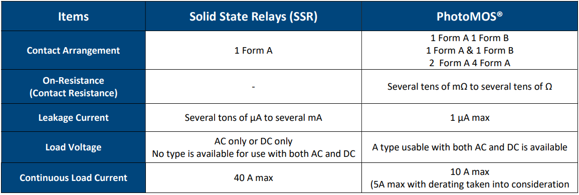
- How can I determine whether to use PhotoMOS® Relays or Solid State Relays (SSR)?
- What is the relationship between the LED operation current and the recommended LED forward current?
- Is it possible to use a DC-only type PhotoMOS® Relay with a negative voltage applied? (Ex: 0 V to pin No. 4 and -12 V to pin No. 3 of AQZ102)
- What are the points to note when selecting a PhotoMOS® Relay for its load voltage?
- What is the definition of operating ambient temperatures of PhotoMOS® Relays and Solid State Relays (SSR) in Panasonic’s catalog?
- What are the two categories of Panasonic’s PhotoMOS® Relays?
- Does Panasonic have products that allow the use of PC board sockets?
- What is the meaning of “LED dropout voltage” in the PhotoMOS® Relay product specifications?
- What is the input voltage range of PhotoMOS® Relays?
- How many times can a reflow process be applied to PhotoMOS® Relays?
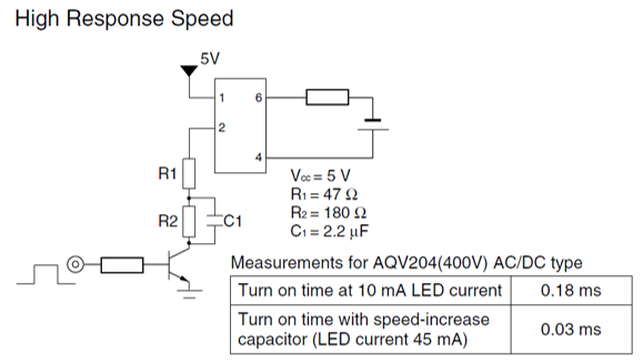
How to shorten the operate/release time of PhotoMOS® relays?
You can shorten the operate/release time by increasing the LED operation current. Note that the LED life will be shortened when doing this.
(If this is used, the input current will increase only during operation, so the life of the LED will be extended.)
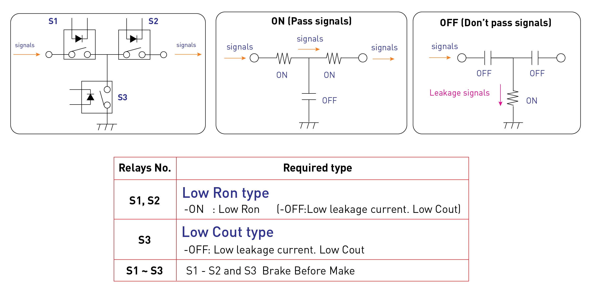
Are PhotoMOS® suitable for Reed Relay Replacement?
PhotoMOS® uses MOS-FET for its output. When compared with the reed relay, there is a characteristic that the capacitance between output terminals is high. Using the circuit shown below, it is possible to reduce the output capacitance between these terminals that may be exaggerated from high-frequency signals.
Higher capacitance values can cause higher frequency signal leakage. Since the PhotoMOS® behaves like a capacitor turned off, high-frequency signals tend to leak. A low C-out type is required when the signal is a high frequency. The above circuit diagram is an example of a “T-type” circuit that creates a way to pass a leakage signal to the GND side when it is OFF.
Read more about using PhotoMOS® for Reed Relay Replacements here.
The peak load current in the rating table is based on 100-ms application (1 shot). Can a higher current be applied if the time is shorter?
No, the peak load current does not increase even if the application time becomes shorter. Ensure that the requirements in the rating table are met.
How should I choose an input-limiting resistor for PhotoMOS® (assuming constant voltage source)?
Please calculate the resistance with the formula shown below.
Calculation Formula
Input-limiting resistance = (Voltage of the voltage source - LED voltage drop) / Current you want to input
Example
The following shows a case of using a 5 V DC constant voltage source at 25°C.
- Voltage: To be calculated by taking the LED voltage drop (1.5 V max) into consideration.
5 V - 1.5 V = 3.5 V
- Current: When the current we recommend is applied [(1) 5 mA or (2) 10 mA], using Ohm's law,
(1) R = 3.5/0.005 = 700 Ω
(2) R = 3.5/0.01 = 350 Ω
Please note that if the LED voltage drop is not taken into consideration, the input current (= If value) becomes lower, and PhotoMOS® may not be able to function correctly.
- You cannot use an AC power supply because a reverse voltage will break the LED (diode).
- If using a wire connection, please carefully check the internal circuit diagram.
A diode is placed in parallel with the output MOSFET. Can it be used as a clamp diode?
The diode placed in parallel with MOSFET is a parasitic diode, formed due to the MOSFET structure. Therefore, general diode performance cannot be guaranteed with this diode.
If you need a clamp diode, an external one should be added.
The catalog does not include the minimum applicable load value. What is the lowest current that can be correctly controlled by PhotoMOS®?
For PhotoMOS®, the minimum applicable load is not specified. PhotoMOS® can correctly function with a current above the off-state leakage current (max) indicated in the catalog. Please note that if the current is close to the off-state leakage current, it may be impossible to turn off the load.
Leakage current: A current that passes (leaks) on the output side even while the input side is off when a specified level of voltage is applied to the output side.
Is it possible to increase the load current value of PhotoMOS® by decreasing the load voltage from the specified absolute maximum rating?
No, it isn't. Due to having characteristics like that of a MOSFET, it is not possible to increase the current value even if the voltage is decreased.
Please be sure to follow the absolute maximum rating specification in the catalog and specifications.
What are the differences among the typical and maximum LED operation currents, and the LED input current?
LED Operation Current
- Typical: The average actual LED current that turns on PhotoMOS®
- Maximum: The maximum actual LED current that turns on PhotoMOS®
LED Operation (Forward) Current
The recommended value of the current to be applied to turn on the PhotoMOS® reliably.
Example: Case of AQY212S
LED operation current: Typical: 0.9 mA / Maximum: 3 mA
Recommended operating condition: LED forward current of 5 mA
After collecting data from many test samples, the average value of the actual LED currents which turned the samples on was 0.9 mA.
The maximum value was 3 mA.
As shown above, the maximum actual current required to turn on the AQY212S was 3 mA, however, we recommend a current of 5 mA to reliably turn it on.
Are there any areas of concern when mounting PhotoMOS® Relays in various orientations?
Unlike Mechanical Relays, Semiconductor Relays (PhotoMOS® or SSR) do not have a moveable contact structure and can be placed in any direction without limitations.
However, ensure a proper PCB arrangement that allows for airflow as a counter-measure against rises in ambient temperature.
Are there any problems when a 1 Form A and 1 Form B contact of a PhotoMOS® is used as a 1 Form C contact?
When a 1 Form A and 1 Form B contact is used as a 1 Form C contact, there are potential problems as shown below.
- The N.O. and N.C. contacts may simultaneously pass a current due to variations in the turn-on and turn-off times among products, temperatures, and current characteristics.
- In addition, there is a small leakage current even when the contact is opened.
Please take the necessary measures to ensure that the circuit prevents the above problems above and carefully check the operation of the relay installed in the actual equipment.
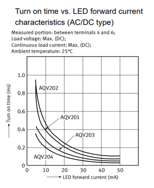
What is the relationship between the LED operation current and the recommended LED forward current?
The typical and maximum current values in Panasonic’s PhotoMOS® catalogs show those at an ambient temperature of 25°C.
The LED operation current increases as the ambient temperature rises.
Below is an example of the LED operation current vs. ambient temperature characteristics (typically shown in the REFERENCE DATA section of our catalogs).
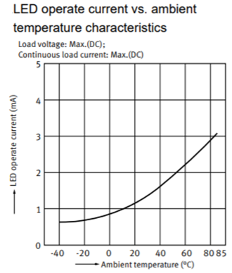
If you set the LED current to the typical approximate value, the operation may be unreliable in an environment with a high ambient temperature.
In consideration of the above, our catalogs show a recommended LED forward current, which is the LED current with which the relay can reliably operate.
Is it possible to use a DC-only type PhotoMOS® Relay with a negative voltage applied? (Ex: 0 V to pin No. 4 and -12 V to pin No. 3 of AQZ102)
There is no problem as long as the potential of pin No. 4 is higher than that of pin No. 3, which means that the current direction is correct.
What are the points to note when selecting a PhotoMOS® Relay for its load voltage?
When selecting a PhotoMOS® Relay for its load voltage, please be careful about the difference between the peak value and the RMS value.
It is also important to take the safety margin into consideration (derating).
For example, the specifications of the GU 1 Form A type are as shown below.
- 400 V AC (peak)
- 400 V DC
What is the definition of operating ambient temperatures of PhotoMOS® Relays and Solid State Relays (SSR) in Panasonic’s catalog?
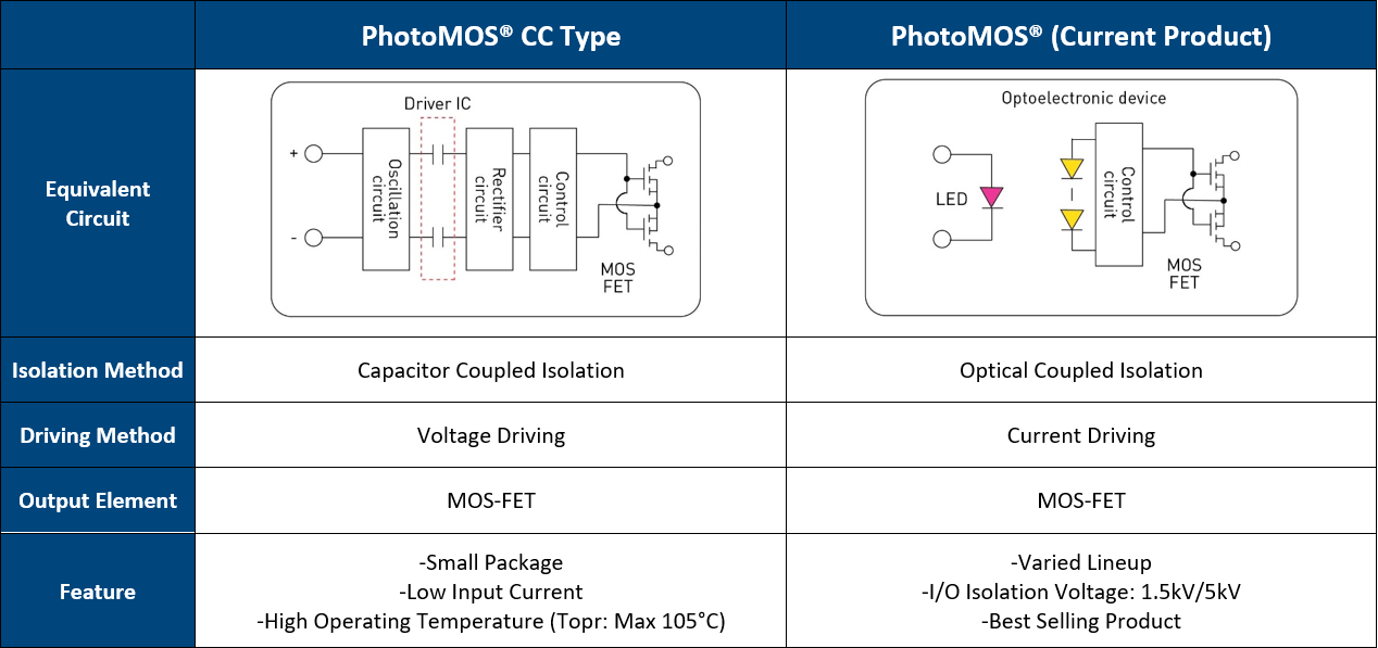
What are the two categories of Panasonic’s PhotoMOS® Relays?
The major difference is their driving and isolation methods (Capacitor Coupled and LED) which are described in the below comparison chart.
Does Panasonic have products that allow the use of PC board sockets?
What is the meaning of “LED dropout voltage” in the PhotoMOS® Relay product specifications?
The LED dropout voltage is a voltage drop across the input terminals caused by a forward current.
When the value of a limiting resistor that determines the LED forward current (IF) is obtained, the LED voltage drop needs to be taken into consideration.
The following relationship holds:
Limiting resistor value = (Power supply voltage - LED voltage drop) / LED current
What is the input voltage range of PhotoMOS® Relays?
Most PhotoMOS® Relays are current-driven. Therefore, voltage values are not specified for the input sides of PhotoMOS® except for a few voltage input types.
Please insert a limiting resistor in series so that the input current becomes equivalent to the recommended current. The necessary resistance value should vary depending on the power supply voltage.
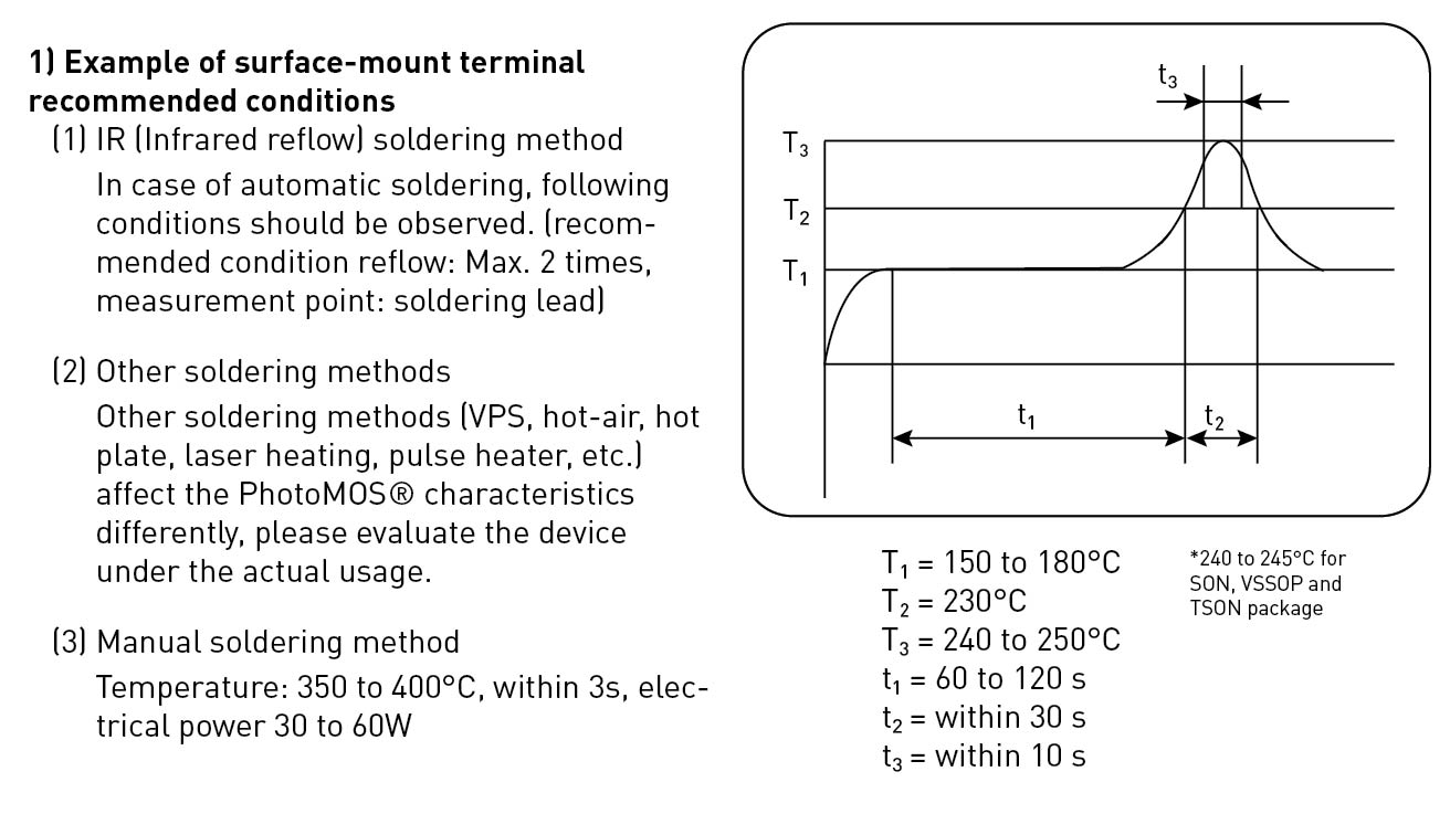
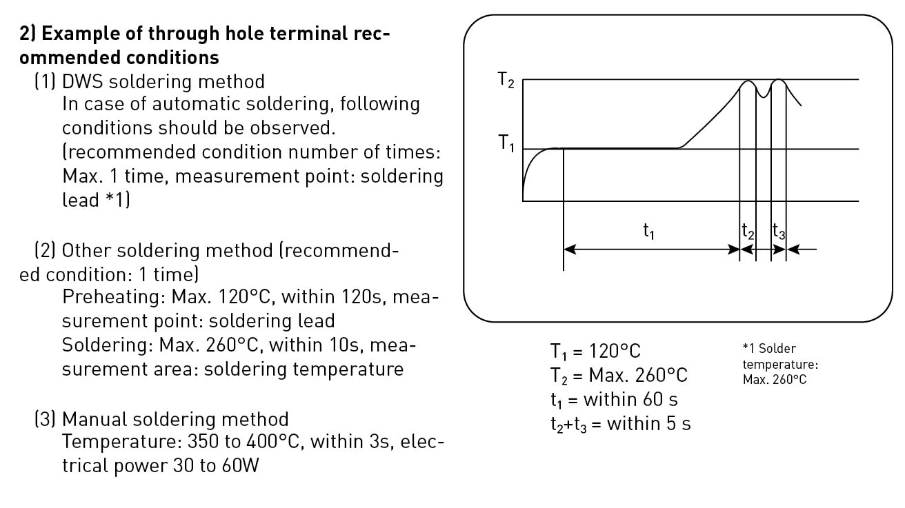
How many times can a reflow process be applied to PhotoMOS® Relays?
Up to two times.
Panasonic’s detailed recommended reflow soldering conditions are described in the “Soldering” section of the catalog “PhotoMOS Cautions for Use.” Please check the catalog for details.