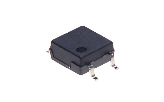
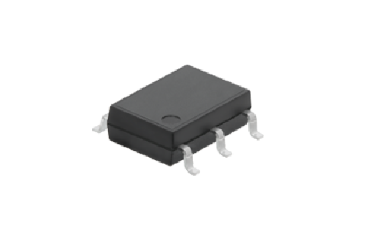
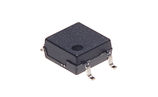
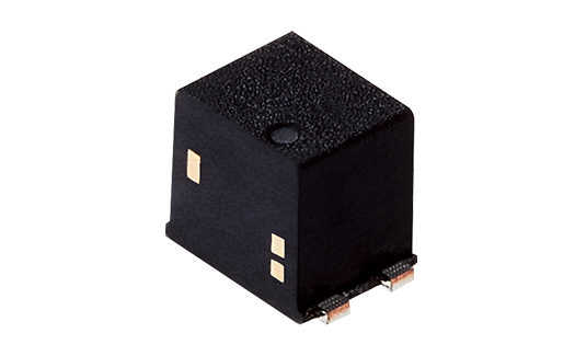
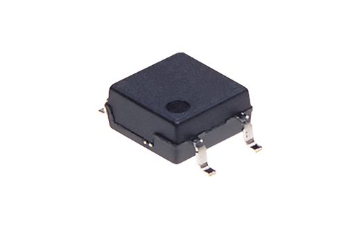
PhotoMOS GU 1 Form A (DIP6-pin type)

PhotoMOS® GU 1 Form A Relay comes in our DIP6-pin package specialized for switching low-level analog signals. This Relay also features stable on-resistance, a low-level off-state leakage current of max. 1uA and reinforced insulation type of 5,000V between input and output. Additionally, this PhotoMOS eliminates the need for a counter electromotive force (EMF) protection diode in the drive circuits on the input side. 

Features and Benefits of PhotoMOS GU 1 Form A

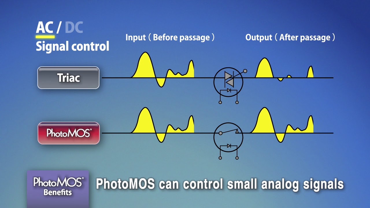
  • Controls Low-Level Analog Signals
  • Controls Various Types Of Loads Such As Relays, Motors, Lamps, And Solenoids
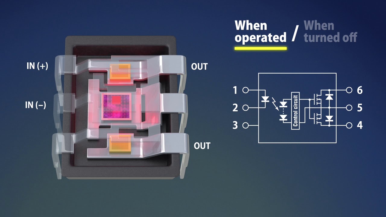
  • Optical Coupling For Extremely High Isolation
  • Eliminates The Need For A Counter Electromotive Force Protection Diode In The Drive Circuits On The Input Side
  • Stable On-Resistance
  • Low-Level Off-State Leakage Current Of Max. 1 μA
  • Reinforced Insulation Type Of I/O voltage 5,000Vrms Is Also Available

PhotoMOS GU 1 Form A Applications

  • High-Speed Inspection Machines
  • Telephone Equipment
  • Data Communication Equipment
  • Computers


Series image for PhotoMOS GU 1 Form A (DIP6-pin type)

PhotoMOS GU 1 Form A (DIP6-pin type)

Part number list

Results 28
Models table for series PhotoMOS GU 1 Form A (DIP6-pin type)
Part No.DatasheetPackageVoltage TypeLoad Voltage [ VL ] (VL)Continuous Load Current (IL)I/O Isolation Voltage (Viso)Terminal TypePacking QuantityProduct NameTypeLED Forward Current (IF)LED Reverse Voltage (VR)Peak Forward Current (IFP)Power Dissipation (Pin)Peak Load Current (Ipeak)Power Dissipation (Pout)Total Power Dissipation (Pt)Ambient Temperature: Operating (Topr)Ambient Temperature: Storage (Tstg)LED Operate Current (Typical) LED Operate Current (Maximum)LED Turn Off Current (Minimum) LED Turn Off Current (Typical) LED Dropout Voltage (Typical) (VF)LED Dropout Voltage (Maximum) (VF)On Resistance (Typical) (Ron)On Resistance (Maximum) (Ron)Off State Leakage Current (Maximum) (ILeak)Over Current ProtectionTurn On Time (Typical) Turn On Time (Maximum) Turn Off Time (Typical)Turn Off Time (Maximum)I/O Capacitance (Typical) (Ciso)I/O Capacitance (Maximum) (Ciso)Initial I/O Isolation Resistance (Minimum) (Riso)LED Current (IF)Load Voltage (VL)Continuous Load Current (IL)Contact ArrangementExternal DimensionsRecommended Mounting Pad (Top View) PC Board Pattern (Bottom View) Load currentJunction temperature (Tj)Packing quantity
1-tube (pcs.)
Packing quantity
Outer carton (pcs.)
Packing quantity
1-reel (pcs.)
DIP6
AC/DC
350 V
0.13 A
1,500 Vrms
Through hole terminal
Tube packing style
GU 1 Form A
GU
50 mA
5 V
1 A
75 mW
0.4 A
500 mW
550 mW
-40 to +85℃
-40 to +100℃
1 mA
3 mA
0.4 mA
0.79 mA
1.25 V
1.5 V
23 Ω
35 Ω
1μA
Nothing
0.25 ms
0.5 ms
0.05 ms
0.2 ms
0.8 pF
1.5 pF
1,000 M ohm
Min.: 5 mA, Max.: 30 mA
Max.: 280 V
Max.: 0.13 A
1 Form A
130 mA
125℃
50
500
DIP6
AC/DC
350 V
0.13 A
1,500 Vrms
Surface-mount terminal
Tape and reel packing style (X)
GU 1 Form A
GU
50 mA
5 V
1 A
75 mW
0.4 A
500 mW
550 mW
-40 to +85℃
-40 to +100℃
1 mA
3 mA
0.4 mA
0.79 mA
1.25 V
1.5 V
23 Ω
35 Ω
1μA
Nothing
0.25 ms
0.5 ms
0.05 ms
0.2 ms
0.8 pF
1.5 pF
1,000 M ohm
Min.: 5 mA, Max.: 30 mA
Max.: 280 V
Max.: 0.13 A
1 Form A
130 mA
125℃
1,000
1,000
DIP6
AC/DC
400 V
0.12 A
1,500 Vrms
Surface-mount terminal
Tape and reel packing style (Z)
GU 1 Form A
GU
50 mA
5 V
1 A
75 mW
0.3 A
500 mW
550 mW
-40 to +85℃
-40 to +100℃
1 mA
3 mA
0.4 mA
0.79 mA
1.25 V
1.5 V
30 Ω
50 Ω
1μA
Nothing
0.21 ms
0.5 ms
0.05 ms
0.2 ms
0.8 pF
1.5 pF
1,000 M ohm
Min.: 5 mA, Max.: 30 mA
Max.: 320 V
Max.: 0.12 A
1 Form A
120 mA
125℃
1,000
1,000
DIP6
AC/DC
400 V
0.12 A
5,000 Vrms
Surface-mount terminal
Tape and reel packing style (Z)
GU 1 Form A
GU
50 mA
5 V
1 A
75 mW
0.3 A
500 mW
550 mW
-40 to +85℃
-40 to +100℃
1 mA
1.3 mA
0.4 mA
1.2 mA
1.25 V
1.5 V
30 Ω
50 Ω
1μA
Nothing
0.6 ms
0.8 ms
0.05 ms
0.2 ms
0.8 pF
1.5 pF
1,000 M ohm
Min.: 5 mA, Max.: 30 mA
Max.: 320 V
Max.: 0.12 A
1 Form A
120 mA
125℃
1,000
1,000
DIP6
AC/DC
100 V
0.32 A
1,500 Vrms
Surface-mount terminal
Tape and reel packing style (Z)
GU 1 Form A
GU
50 mA
5 V
1 A
75 mW
0.96 A
500 mW
550 mW
-40 to +85℃
-40 to +100℃
1 mA
3 mA
0.4 mA
0.79 mA
1.25 V
1.5 V
2.3 Ω
4.0 Ω
1μA
Nothing
0.60 ms
2 ms
0.06 ms
0.2 ms
0.8 pF
1.5 pF
1,000 M ohm
Min.: 5 mA, Max.: 30 mA
Max.: 80 V
Max.: 0.3 A
1 Form A
320 mA
125℃
1,000
1,000
DIP6
AC/DC
600 V
0.05 A
1,500 Vrms
Surface-mount terminal
Tape and reel packing style (Z)
GU 1 Form A
GU
50 mA
5 V
1 A
75 mW
0.15 A
500 mW
550 mW
-40 to +85℃
-40 to +100℃
1 mA
3 mA
0.4 mA
0.79 mA
1.25 V
1.5 V
70 Ω
120 Ω
1μA
Nothing
0.28 ms
0.5 ms
0.04 ms
0.2 ms
0.8 pF
1.5 pF
1,000 M ohm
Min.: 5 mA, Max.: 30 mA
Max.: 480 V
Max.: 0.05 A
1 Form A
50 mA
125℃
1,000
1,000
DIP6
AC/DC
60 V
0.55 A
1,500 Vrms
Surface-mount terminal
Tube packing style
GU 1 Form A
GU
50 mA
5 V
1 A
75 mW
1.5 A
500 mW
550 mW
-40 to +85℃
-40 to +100℃
1 mA
3 mA
0.4 mA
0.79 mA
1.25 V
1.5 V
0.83 Ω
2.5 Ω
1μA
Nothing
0.65 ms
2 ms
0.08 ms
0.2 ms
0.8 pF
1.5 pF
1,000 M ohm
Min.: 5 mA, Max.: 30 mA
Max.: 48 V
Max.: 0.5 A
1 Form A
550 mA
125℃
50
500
DIP6
AC/DC
100 V
0.32 A
1,500 Vrms
Surface-mount terminal
Tube packing style
GU 1 Form A
GU
50 mA
5 V
1 A
75 mW
0.96 A
500 mW
550 mW
-40 to +85℃
-40 to +100℃
1 mA
3 mA
0.4 mA
0.79 mA
1.25 V
1.5 V
2.3 Ω
4.0 Ω
1μA
Nothing
0.60 ms
2 ms
0.06 ms
0.2 ms
0.8 pF
1.5 pF
1,000 M ohm
Min.: 5 mA, Max.: 30 mA
Max.: 80 V
Max.: 0.3 A
1 Form A
320 mA
125℃
50
500
DIP6
AC/DC
600 V
0.05 A
1,500 Vrms
Surface-mount terminal
Tube packing style
GU 1 Form A
GU
50 mA
5 V
1 A
75 mW
0.15 A
500 mW
550 mW
-40 to +85℃
-40 to +100℃
1 mA
3 mA
0.4 mA
0.79 mA
1.25 V
1.5 V
70 Ω
120 Ω
1μA
Nothing
0.28 ms
0.5 ms
0.04 ms
0.2 ms
0.8 pF
1.5 pF
1,000 M ohm
Min.: 5 mA, Max.: 30 mA
Max.: 480 V
Max.: 0.05 A
1 Form A
50 mA
125℃
50
500
Latest Videos

Playlist

Thumbnail for Features and Benefits of PhotoMOS®

Features and Benefits of PhotoMOS®

Thumbnail for Introduction to PhotoMOS®

Introduction to PhotoMOS®

Thumbnail for New Product Spotlight: PhotoMOS® HE 1 Form A and HE SOP 1 Form A Series Relays
New Product Spotlight: PhotoMOS® HE 1 Form A and HE SOP 1 Form A Series Relays

Thumbnail for NPI: PhotoMOS® HF 1 Form A Series High Capacity Relays
NPI: PhotoMOS® HF 1 Form A Series High Capacity Relays

Thumbnail for NPI: Photovoltaic MOSFET PhotoMOS® Relays
NPI: Photovoltaic MOSFET PhotoMOS® Relays

Thumbnail for New Product Brief: Photovoltaic MOSFET Driver High Power Type
New Product Brief: Photovoltaic MOSFET Driver High Power Type

Thumbnail for NPI: PhotoMOS HF 1 Form A High Capacity Relays
NPI: PhotoMOS HF 1 Form A High Capacity Relays

Thumbnail for NPI: PhotoMOS CC TSON 1 Form B

NPI: PhotoMOS CC TSON 1 Form B

Thumbnail for NPI: AQY215S PhotoMOS® Relays
NPI: AQY215S PhotoMOS® Relays
Thumbnail for New Product Introduction: PhotoMOS® GU SOP 1 Form A High-Capacity Semiconductor Relay

New Product Introduction: PhotoMOS® GU SOP 1 Form A High-Capacity Semiconductor Relay