PhotoMOS RF SOP 4 Form A CxR10 Voltage-sensitive

Panasonic's PhotoMOS® RF SOP 4 Form A are characterized by their high performance and 4-channel Form A in a small SOP16-pin package. With RF SOP 4 Form A arrangement these Semiconductor relays are ideal for measuring and testing equipment, communication and broadcasting equipment, medical equipment, multi-point recorders, and more. These devices are equipped with built-in resistors which means fewer man-hours when mounting. Additionally, this device saves space on the PC board and has both low on-resistance and low output capacitance.

Features and Benefits

  • Built-In Input Resistor
  • Saves Space on PC Board
  • Both Low On-Resistance (R type) and Low Capacitance (C type) Available

Applications

  • Measuring and Testing Equipment
  • Telecommunication and Broadcasting Equipment
  • Medical Equipment
  • Multi-Point Recorder
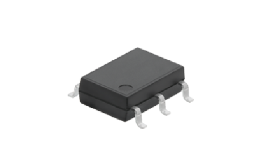
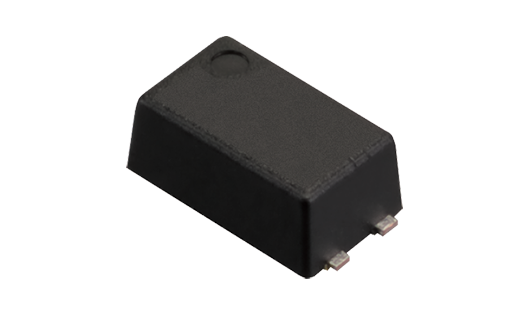
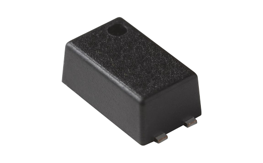
Series image for PhotoMOS RF SOP 4 Form A CxR10 Voltage-sensitive

PhotoMOS RF SOP 4 Form A CxR10 Voltage-sensitive

Part number list

Results 6
Models table for series PhotoMOS RF SOP 4 Form A CxR10 Voltage-sensitive
Part No.DatasheetPackageVoltage TypeLoad Voltage [ VL ] (VL)Continuous Load Current (IL)I/O Isolation Voltage (Viso)Packing QuantityProduct NameTypeInput Voltage (VIN)Input Reverse Voltage (VRIN)Power Dissipation (Pin)Peak Load Current (Ipeak)Power Dissipation (Pout)Total Power Dissipation (Pt)Ambient Temperature: Operating (Topr)Ambient Temperature: Storage (Tstg)Operate Voltage (Typical) (VFon)Operate Voltage (Maximum) (VFon)Turn Off Voltage (Minimum) (VFoff)Turn Off Voltage (Typical) (VFoff)Input Current (Typical) (IIN)On Resistance (Typical) (Ron)On Resistance (Maximum) (Ron)Output Capacitance (Typical) (Cout)Output Capacitance (Maximum) (Cout)Off State Leakage Current (Typical) (ILeak)Off State Leakage Current (Maximum) (ILeak)Over Current ProtectionTurn On Time (Typical) Turn On Time (Maximum) Turn Off Time (Typical)Turn Off Time (Maximum)I/O Capacitance (Typical) (Ciso)I/O Capacitance (Maximum) (Ciso)Initial I/O Isolation Resistance (Minimum) (Riso)Input Voltage (VIN)Load Voltage (VL)Continuous Load Current (IL)Terminal TypeContact ArrangementExternal DimensionsRecommended Mounting Pad (Top View) Load currentJunction temperature (Tj)Packing quantity
1-tube (pcs.)
Packing quantity
Outer carton (pcs.)
Packing quantity
1-reel (pcs.)
SOP16
AC/DC
40 V
0.06 A
500 Vrms
Tape and reel packing style (Z)
RF SOP 4 Form A CxR10 Voltage-sensitive
RF
6 V
5 V
260 mW
0.12 A
600 mW
650 mW
-40 to +85°C
-40 to +100°C
1.3 V
4 V
0.8 V
1.3 V
8.5 mA
9.5 ohm
12.5 ohm
1 pF
1.5 pF
0.01 nA
10 nA
Nothing
0.02 ms
0.5 ms
0.02 ms
0.2 ms
0.8 pF
1.5 pF
1,000 M ohm
Min.: 4.5 V, Max.: 5.5 V
Max.: 15 V
Max.: 0.06 A
Surface-mount terminal
4 Form A
0.06 A
125°C
1,000
1,000
SOP16
AC/DC
40 V
0.16 A
500 Vrms
Tape and reel packing style (X)
RF SOP 4 Form A CxR10 Voltage-sensitive
RF
6 V
5 V
260 mW
0.2 A
600 mW
650 mW
-40 to +85°C
-40 to +100°C
1.3 V
4 V
0.8 V
1.3 V
8.5 mA
0.75 ohm
1.25 ohm
12.5 pF
18 pF
0.02 nA
10 nA
Nothing
0.07 ms
0.5 ms
0.07 ms
0.2 ms
0.8 pF
1.5 pF
1,000 M ohm
Min.: 4.5 V, Max.: 5.5 V
Max.: 15 V
Max.: 0.16 A
Surface-mount terminal
4 Form A
0.16 A
125°C
1,000
1,000
SOP16
AC/DC
40 V
0.06 A
500 Vrms
Tube packing style
RF SOP 4 Form A CxR10 Voltage-sensitive
RF
6 V
5 V
260 mW
0.12 A
600 mW
650 mW
-40 to +85°C
-40 to +100°C
1.3 V
4 V
0.8 V
1.3 V
8.5 mA
9.5 ohm
12.5 ohm
1 pF
1.5 pF
0.01 nA
10 nA
Nothing
0.02 ms
0.5 ms
0.02 ms
0.2 ms
0.8 pF
1.5 pF
1,000 M ohm
Min.: 4.5 V, Max.: 5.5 V
Max.: 15 V
Max.: 0.06 A
Surface-mount terminal
4 Form A
0.06 A
125°C
50
1,000
SOP16
AC/DC
40 V
0.06 A
500 Vrms
Tape and reel packing style (X)
RF SOP 4 Form A CxR10 Voltage-sensitive
RF
6 V
5 V
260 mW
0.12 A
600 mW
650 mW
-40 to +85°C
-40 to +100°C
1.3 V
4 V
0.8 V
1.3 V
8.5 mA
9.5 ohm
12.5 ohm
1 pF
1.5 pF
0.01 nA
10 nA
Nothing
0.02 ms
0.5 ms
0.02 ms
0.2 ms
0.8 pF
1.5 pF
1,000 M ohm
Min.: 4.5 V, Max.: 5.5 V
Max.: 15 V
Max.: 0.06 A
Surface-mount terminal
4 Form A
0.06 A
125°C
1,000
1,000
SOP16
AC/DC
40 V
0.16 A
500 Vrms
Tape and reel packing style (Z)
RF SOP 4 Form A CxR10 Voltage-sensitive
RF
6 V
5 V
260 mW
0.2 A
600 mW
650 mW
-40 to +85°C
-40 to +100°C
1.3 V
4 V
0.8 V
1.3 V
8.5 mA
0.75 ohm
1.25 ohm
12.5 pF
18 pF
0.02 nA
10 nA
Nothing
0.07 ms
0.5 ms
0.07 ms
0.2 ms
0.8 pF
1.5 pF
1,000 M ohm
Min.: 4.5 V, Max.: 5.5 V
Max.: 15 V
Max.: 0.16 A
Surface-mount terminal
4 Form A
0.16 A
125°C
1,000
1,000
SOP16
AC/DC
40 V
0.16 A
500 Vrms
Tube packing style
RF SOP 4 Form A CxR10 Voltage-sensitive
RF
6 V
5 V
260 mW
0.2 A
600 mW
650 mW
-40 to +85°C
-40 to +100°C
1.3 V
4 V
0.8 V
1.3 V
8.5 mA
0.75 ohm
1.25 ohm
12.5 pF
18 pF
0.02 nA
10 nA
Nothing
0.07 ms
0.5 ms
0.07 ms
0.2 ms
0.8 pF
1.5 pF
1,000 M ohm
Min.: 4.5 V, Max.: 5.5 V
Max.: 15 V
Max.: 0.16 A
Surface-mount terminal
4 Form A
0.16 A
125°C
50
1,000
Latest Videos

Playlist

Thumbnail for Features and Benefits of PhotoMOS®

Features and Benefits of PhotoMOS®

Thumbnail for Introduction to PhotoMOS®

Introduction to PhotoMOS®

Thumbnail for New Product Spotlight: PhotoMOS® HE 1 Form A and HE SOP 1 Form A Series Relays
New Product Spotlight: PhotoMOS® HE 1 Form A and HE SOP 1 Form A Series Relays

Thumbnail for NPI: PhotoMOS® HF 1 Form A Series High Capacity Relays
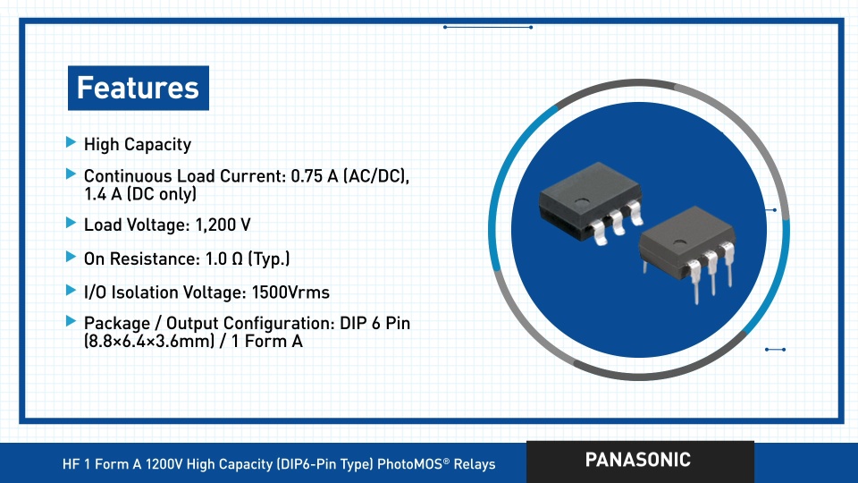
NPI: PhotoMOS® HF 1 Form A Series High Capacity Relays

Thumbnail for NPI: Photovoltaic MOSFET PhotoMOS® Relays
NPI: Photovoltaic MOSFET PhotoMOS® Relays

Thumbnail for New Product Brief: Photovoltaic MOSFET Driver High Power Type
New Product Brief: Photovoltaic MOSFET Driver High Power Type

Thumbnail for NPI: PhotoMOS HF 1 Form A High Capacity Relays
NPI: PhotoMOS HF 1 Form A High Capacity Relays

Thumbnail for NPI: PhotoMOS CC TSON 1 Form B

NPI: PhotoMOS CC TSON 1 Form B

Thumbnail for NPI: AQY215S PhotoMOS® Relays
NPI: AQY215S PhotoMOS® Relays
Thumbnail for New Product Introduction: PhotoMOS® GU SOP 1 Form A High-Capacity Semiconductor Relay

New Product Introduction: PhotoMOS® GU SOP 1 Form A High-Capacity Semiconductor Relay