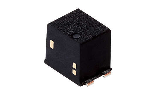
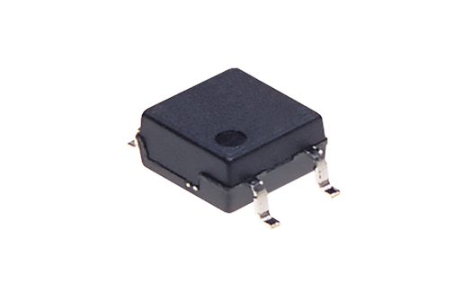
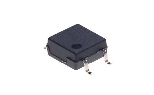
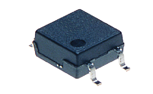
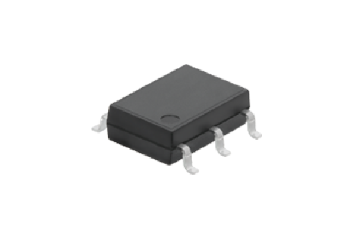
PhotoMOS GU DIP8 1 Form A & 1 Form B
Panasonic’s GU 1 Form A & 1 Form B PhotoMOS® Relay come equipped with both normally open and normally closed contacts integrated into a DIP8-pin package. This Relay provides approximately 50% space savings when compared to mounting a set of 1 Form A and 1 Form B PhotoMOS separately. Additionally, this device can be applied for 1 Form A and 1 Form B use or used independently of one another.
Features and Benefits of PhotoMOS GU 1 Form A & 1 Form B Relay
- Applicable For 1 Form A and 1 Form B Use As Well As Two Independent 1 Form A and 1 Form B Use
- Controls Load Currents Up To 0.13 A With 5 mA Input Current
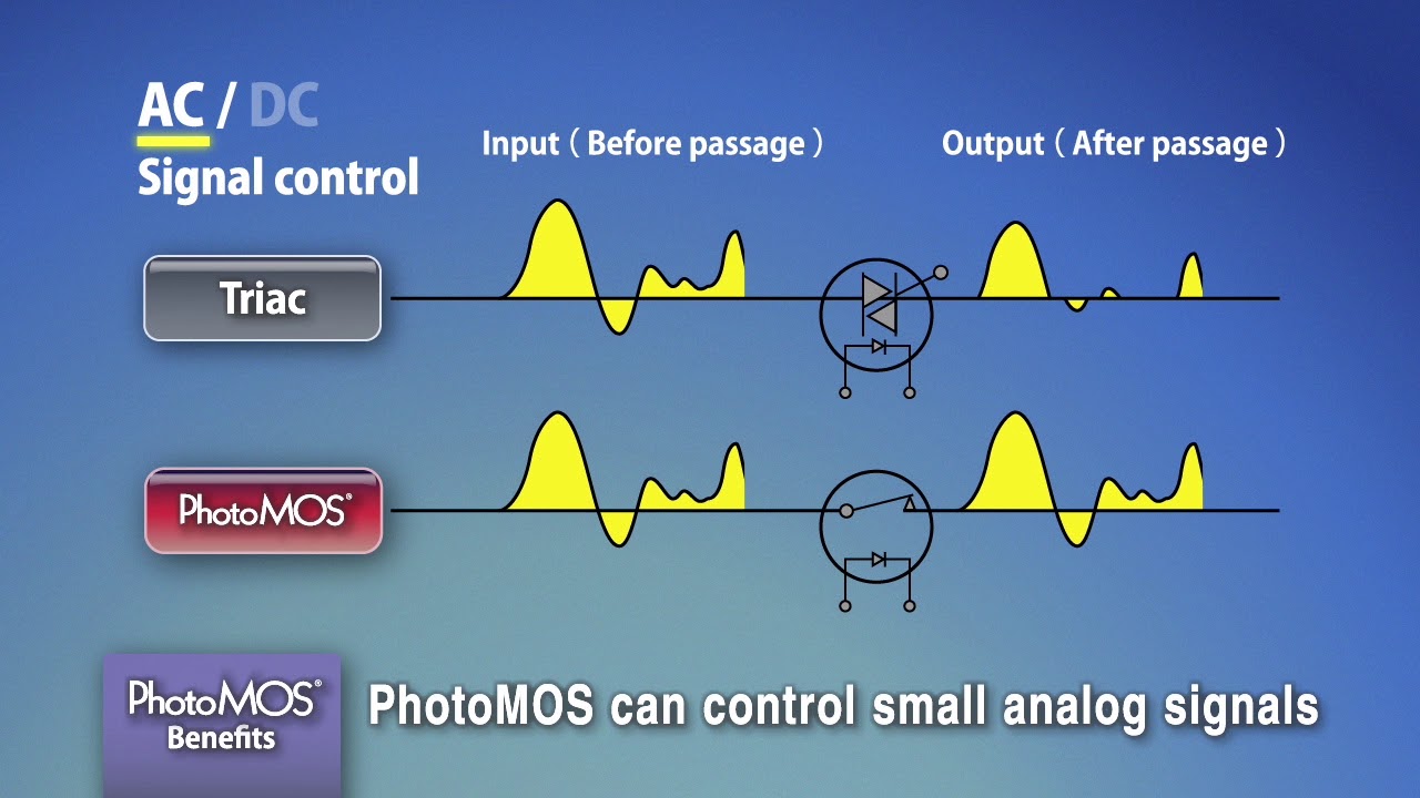
- Extremely Low Closed-Circuit Offset Voltages To Enable Control Of Small Analog Signals Without Distortion
- Stable On-Resistance
PhotoMOS GU 1 Form A & 1 Form B Relay Applications
- High-Speed Inspection Machines
- Telephone Equipment
- Computers
- Sensing Equipment
PhotoMOS GU DIP8 1 Form A & 1 Form B
Part number list
Results 4


Resources
Filter by:
Showing 1 to 10 of 18 results
Results18
What's New
Stay up to date


Latest Videos
Playlist
Features and Benefits of PhotoMOS®
Introduction to PhotoMOS®
New Product Spotlight: PhotoMOS® HE 1 Form A and HE SOP 1 Form A Series Relays
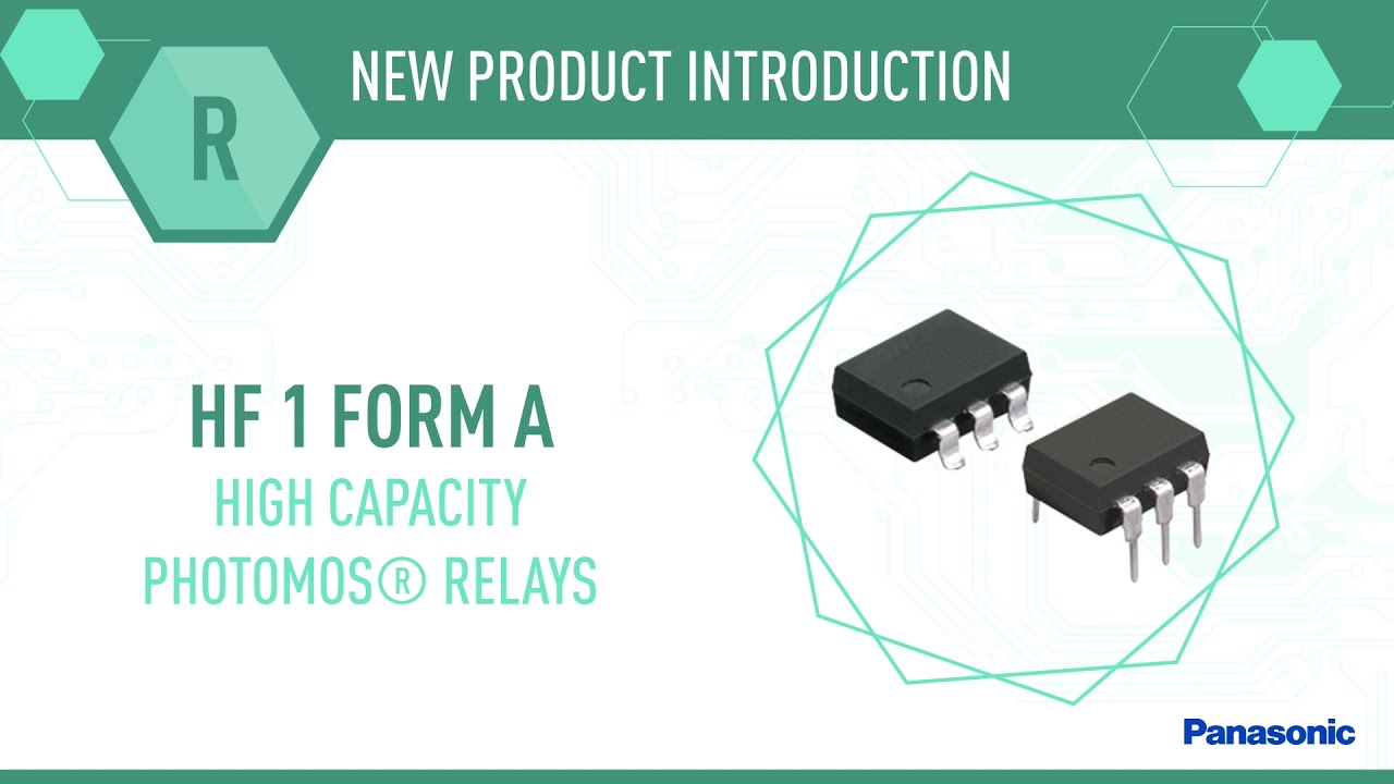
NPI: PhotoMOS® HF 1 Form A Series High Capacity Relays
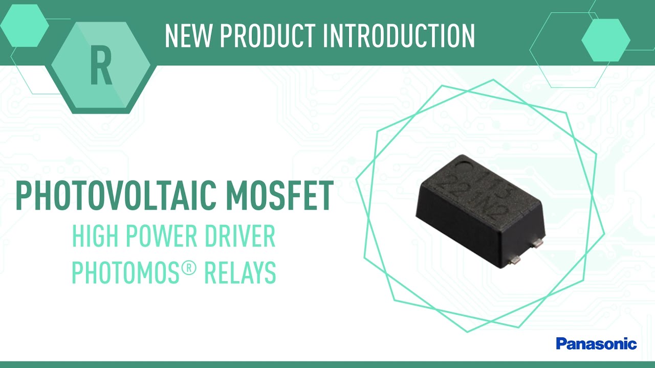
NPI: Photovoltaic MOSFET PhotoMOS® Relays
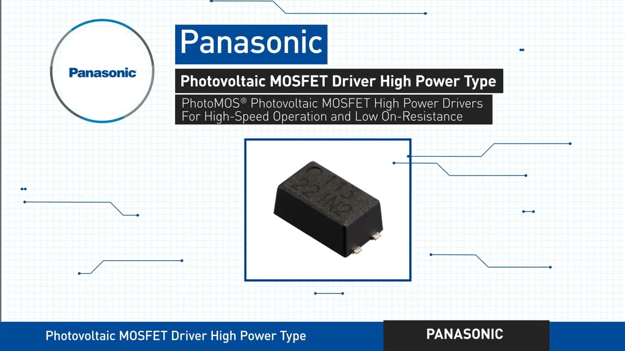
New Product Brief: Photovoltaic MOSFET Driver High Power Type
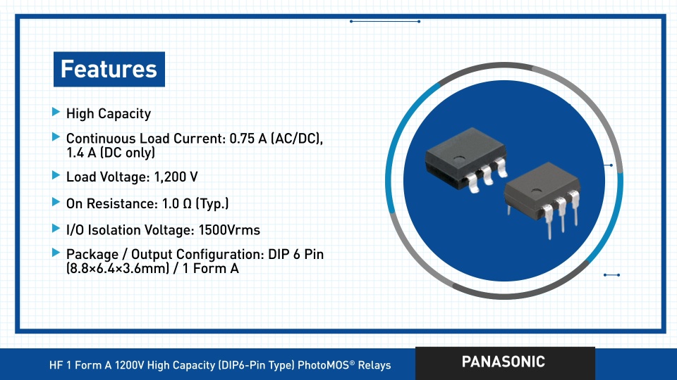
NPI: PhotoMOS HF 1 Form A High Capacity Relays
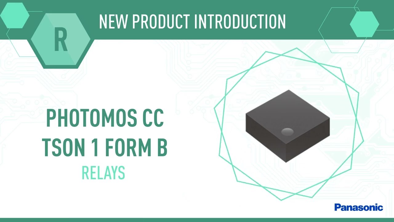
NPI: PhotoMOS CC TSON 1 Form B
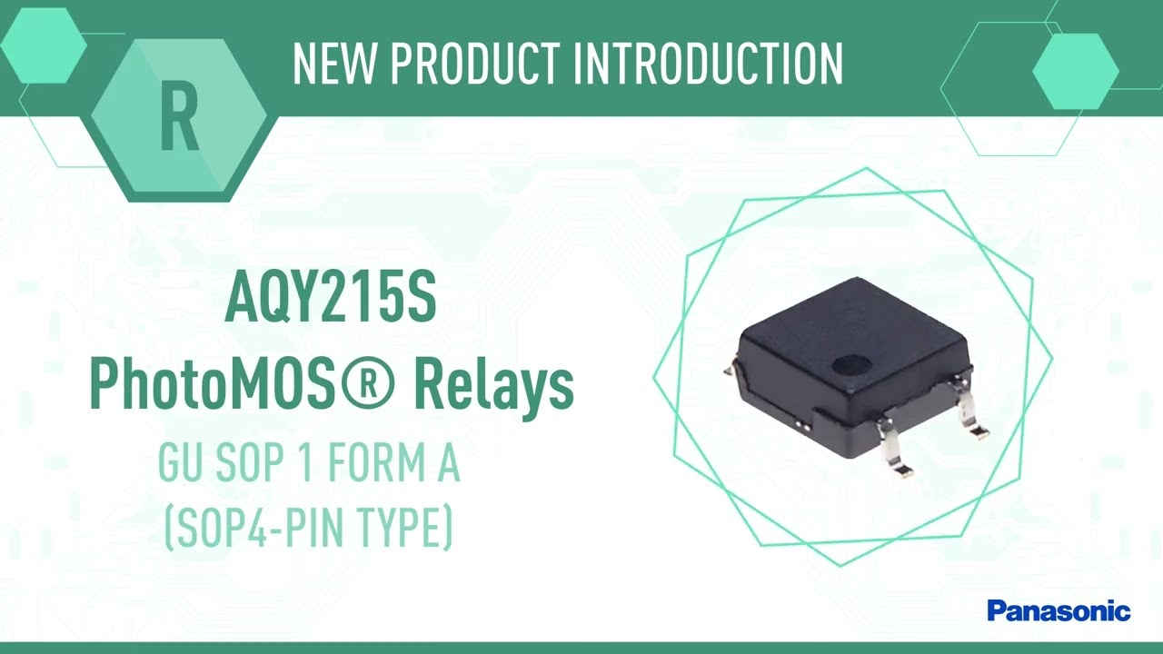
NPI: AQY215S PhotoMOS® Relays