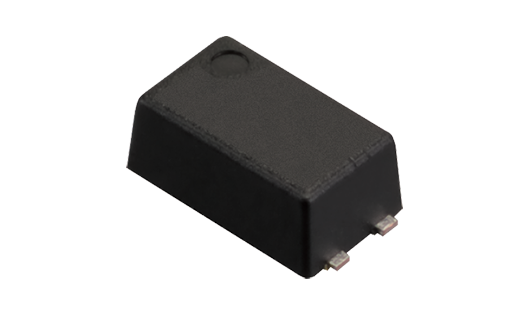
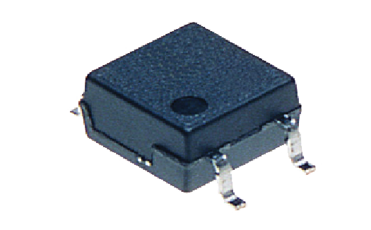
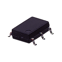
PhotoMOS GU DIP8 2 Form A Current Limiting
The Panasonic PhotoMOS® GU 2 Form A features current limiting capabilities that protect the device from overflow by maintaining a constant output current value when the current reaches a specified limited value in our DIP8-Pin package. This device enhances the capability of surge resistance between output terminals and comes equipped with reinforced insulation of 5,000V. Applicable for both 2 Form A and for two independent 1 Form A uses, this PhotoMOS® is suitable for controlling low-level analog signals, high-speed response times, and low-level off-state leakage current. The typical application for this Relay includes modem and telephone equipment.
Features and Benefits of The PhotoMOS GU 2 Form A Relay
- High I/O Isolation Voltage of 5,000 Vrms
- Current Limiting Function
- 8-Pin Dip Size
- High-Speed Response
- Low-Level Off-State Leakage Current
- Enhances the Capability of Surge Resistance Between Output Terminals
Typical Applications
- Modem
- Telephone Equipment
PhotoMOS GU DIP8 2 Form A Current Limiting
Part number list
Results 4


Resources
Filter by:
Showing 1 to 10 of 15 results
Results15
What's New
Stay up to date

Latest Videos
Playlist
Features and Benefits of PhotoMOS®
Introduction to PhotoMOS®
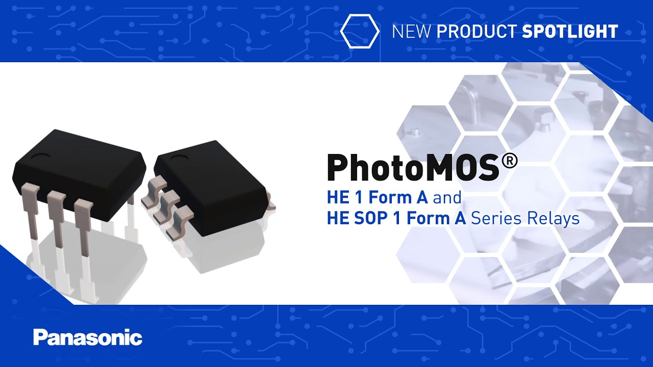
New Product Spotlight: PhotoMOS® HE 1 Form A and HE SOP 1 Form A Series Relays
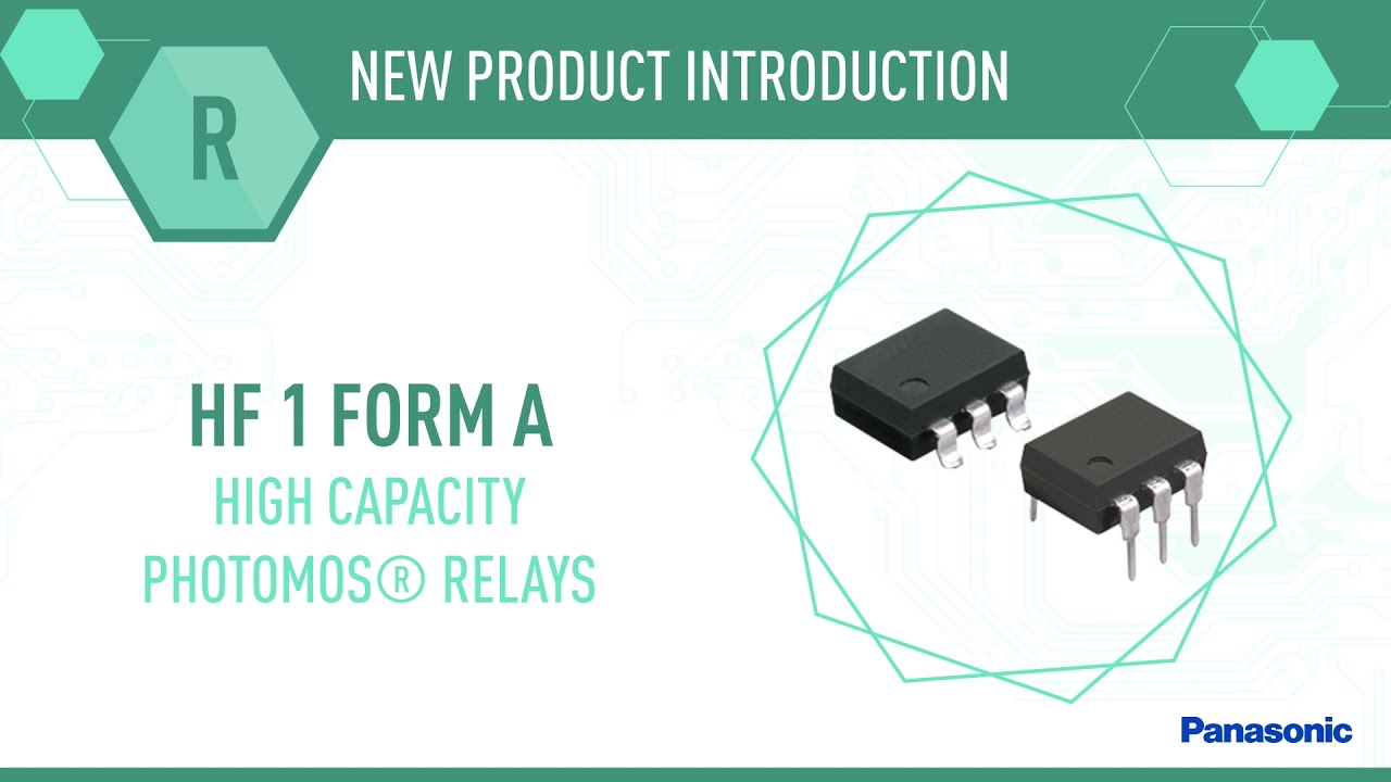
NPI: PhotoMOS® HF 1 Form A Series High Capacity Relays
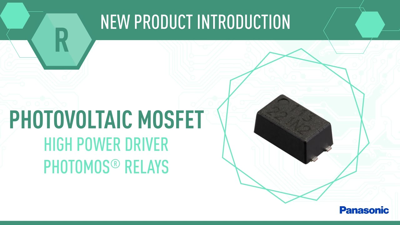
NPI: Photovoltaic MOSFET PhotoMOS® Relays
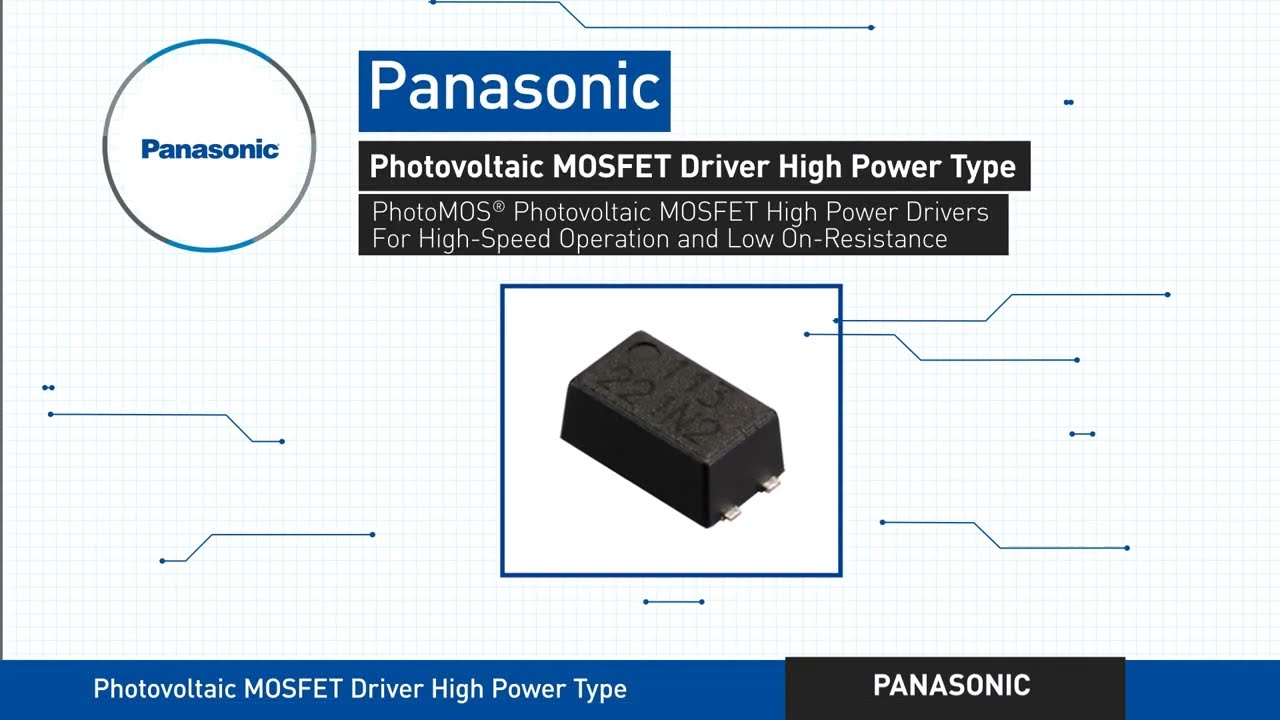
New Product Brief: Photovoltaic MOSFET Driver High Power Type
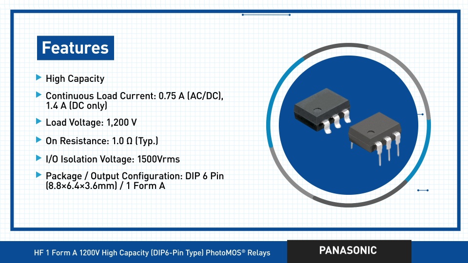
NPI: PhotoMOS HF 1 Form A High Capacity Relays
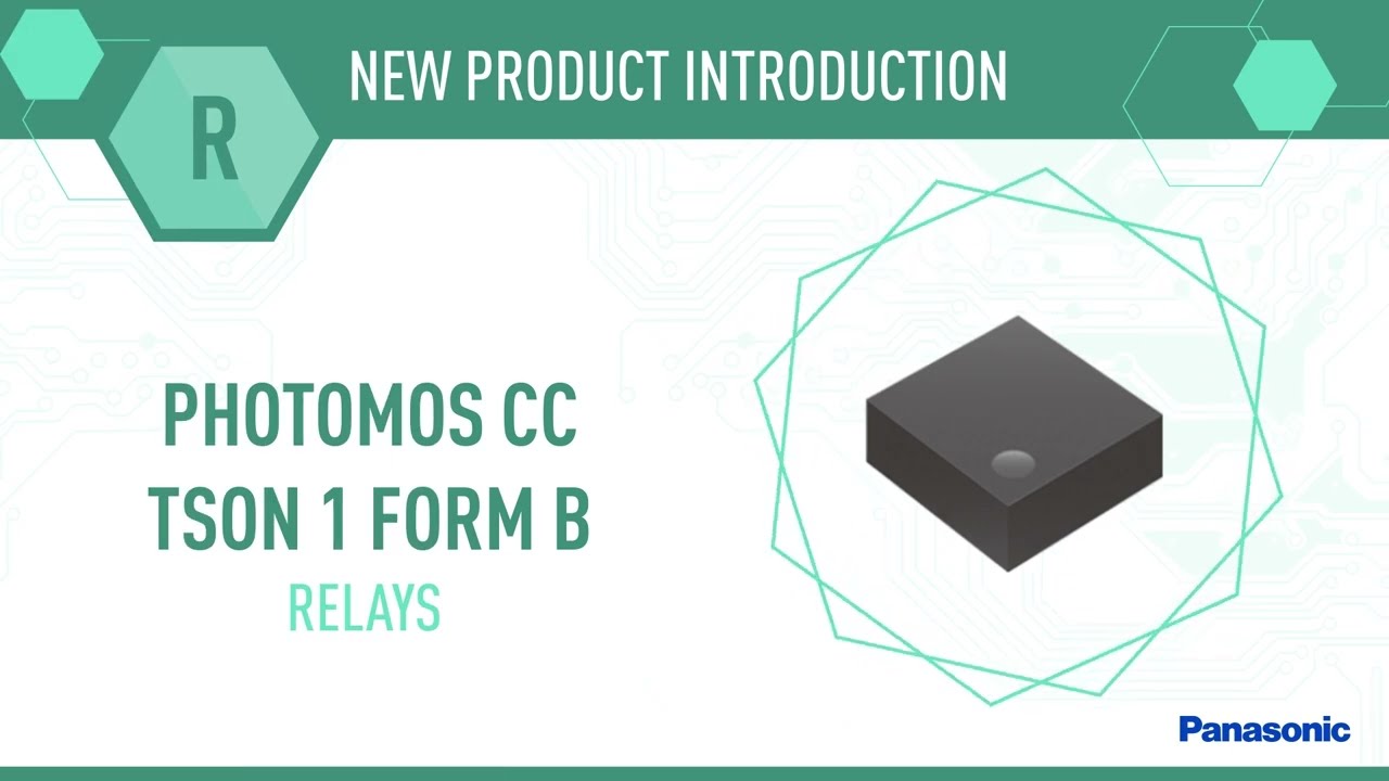
NPI: PhotoMOS CC TSON 1 Form B
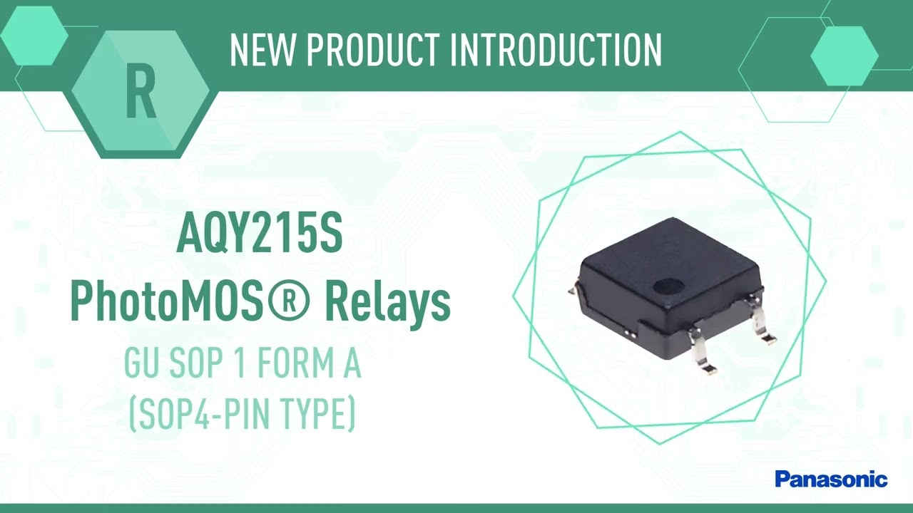
NPI: AQY215S PhotoMOS® Relays