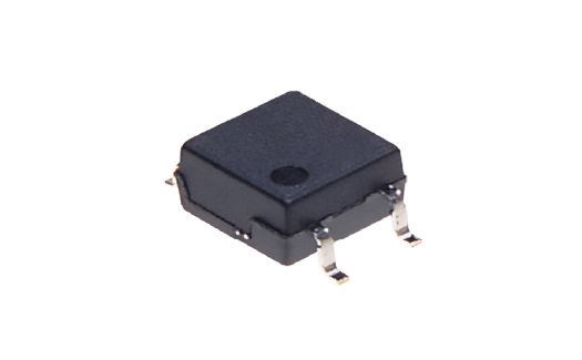
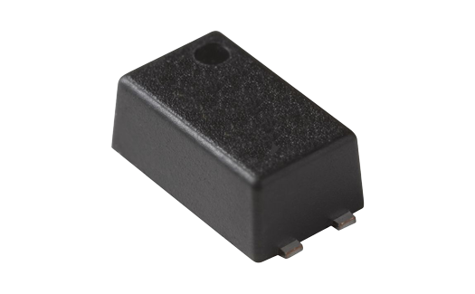
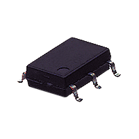
PhotoMOS RF DIP8 2 Form A
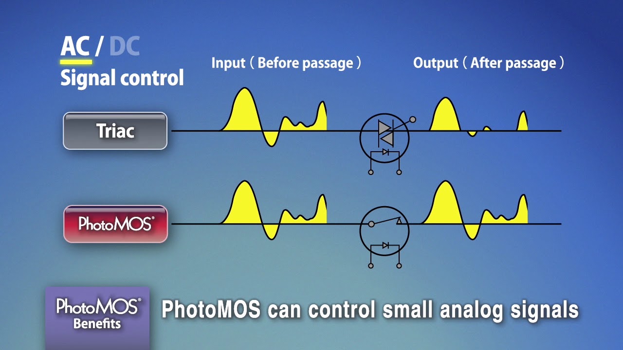
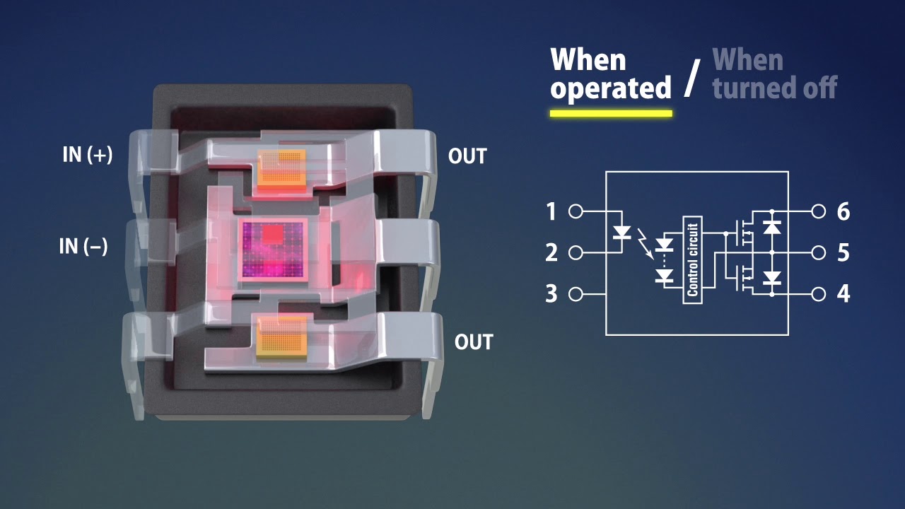
Panasonic's PhotoMOS® RF 2 Form A low on-resistance Relays are available in 8 pin DIP 200V/400V load voltage 2-channels Form A with high response speed, low leakage current, and low on-resistance. Applicable for 2 form A use as well as two independent 1 Form A use. The low capacitance between output terminals ensures high response speed. typically 10pF for typical speed 0.2ms with high sensitivity and low on-resistance. Low-level off-state leakage current. Controls low-level analog signals.
Features and Benefits of PhotoMOS RF 2 Form A low on-resistance
- 2-Channels (Form A) Type With High Response Speed, Low Leakage Current, And Low On-Resistance.
- The Low Capacitance Between Output Terminals Ensures High Response Speed
- High Sensitivity And Low On-Resistance
- Low-Level Off-State Leakage Current
- Controls Low-Level Analog Signals
PhotoMOS RF 2Form A low on-resistance Applications
- Measuring Instruments
- Telephones
- Computer Input Machines
- Industrial Robots
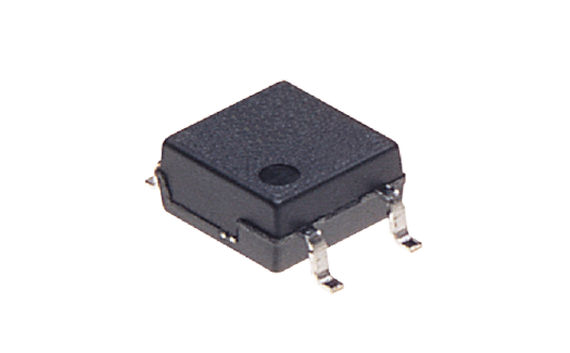
PhotoMOS RF DIP8 2 Form A
Part number list
Results 8


Resources
Filter by:
Showing 1 to 10 of 16 results
Results16
What's New
Stay up to date

Latest Videos
Playlist
Features and Benefits of PhotoMOS®
Introduction to PhotoMOS®

New Product Spotlight: PhotoMOS® HE 1 Form A and HE SOP 1 Form A Series Relays
NPI: PhotoMOS® HF 1 Form A Series High Capacity Relays
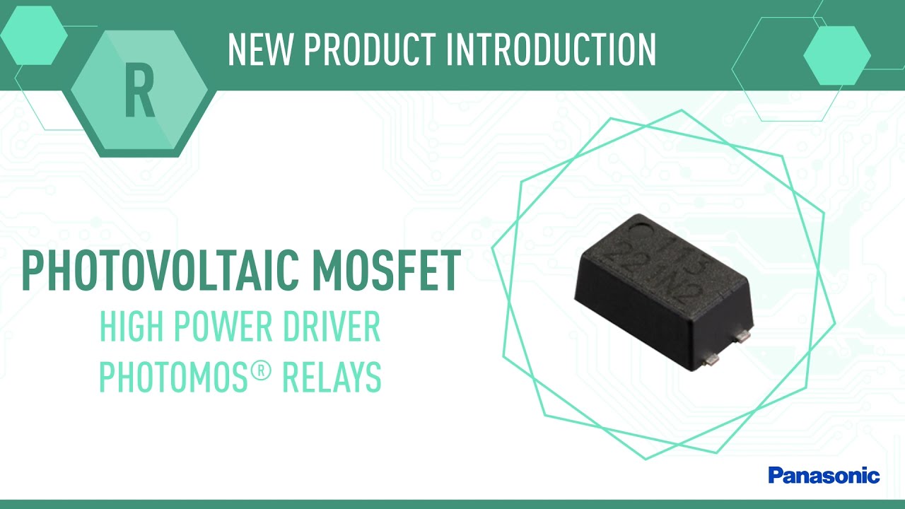
NPI: Photovoltaic MOSFET PhotoMOS® Relays
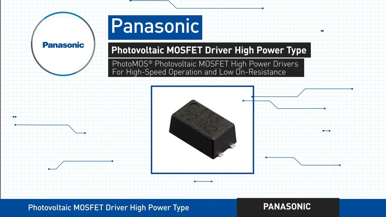
New Product Brief: Photovoltaic MOSFET Driver High Power Type
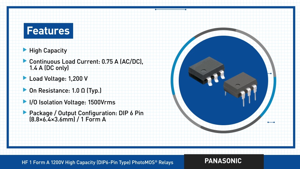
NPI: PhotoMOS HF 1 Form A High Capacity Relays
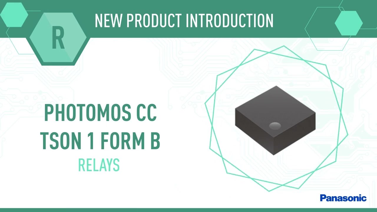
NPI: PhotoMOS CC TSON 1 Form B
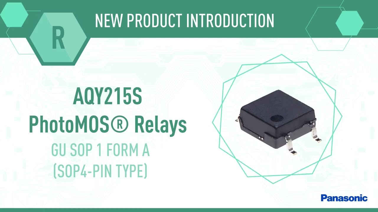
NPI: AQY215S PhotoMOS® Relays