PhotoMOS HS WSSOP 1 Form A Low C x R
PhotoMOS® HS WSSOP 1 Form A Low C x R Semiconductor Relays
Suitable for Test and Measurement Applications with an Extremely Small Footprint, Low Current Consumption, High Ambient Operating Temperature, and Excellent High-Frequency Passing Characteristics!
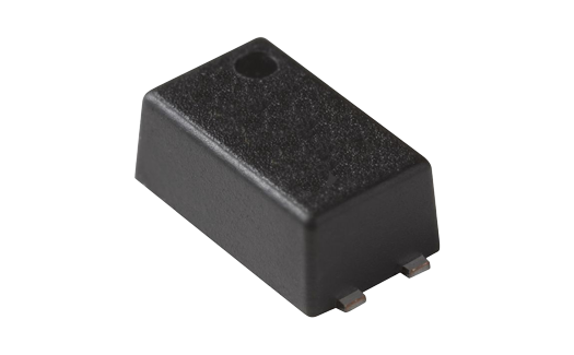
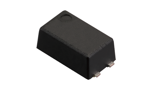
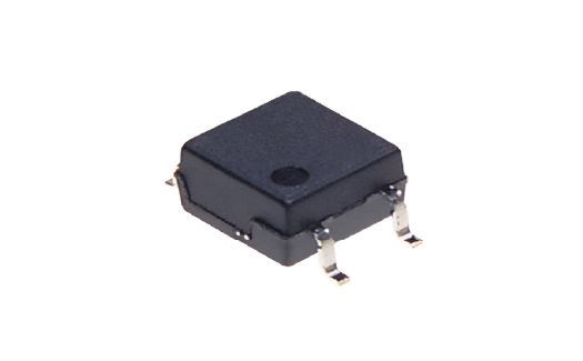
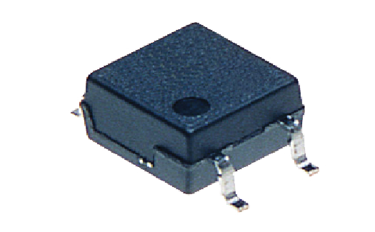
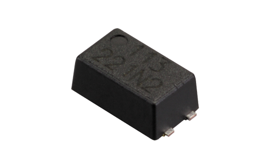
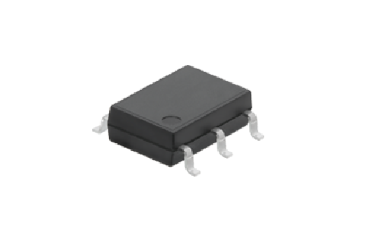
Panasonic’s PhotoMOS® HS WSSOP 1 Form A Low C x R Semiconductor Relays come in a miniature WSSOP package of 1.45 x 2.2 x 1.75mm for high-density mounting. The new PhotoMOS® HS WSSOP device also features low current consumption, high-speed operating temperatures, fast switching speeds, and excellent high-frequency passing characteristics such as low Output Capacitance and low On-Resistance.
The PhotoMOS® HS WSSOP Semiconductor Relays have low leakage of 10nA, typical output capacitance of 16pF, and typical On-Resistance of 0.75 Ohms. With a load output rating at 40V and 0.35A, this Semiconductor Relay is suitable for IC testers, board testers, probe cards, and other measuring equipment.
Features and Benefits
- Miniature WSSOP Package for High-Density Mounting
- Low Current Consumption of 0.15mA for Energy Savings
- High Operating Temperature Performance of 125° C
- High Switching Speeds at 0.025ms for Increased Throughput Capacity
Industries
- Test and Measurement
- Telecommunication
- Factory Automation
Applications
- IC Tester, Probe Card, Board Tester
- Telecommunication Equipment
- Industrial Equipment
PhotoMOS HS WSSOP 1 Form A Low C x R
Part number list
Resources
New Product Information Download

<p>Find the latest new product details here, with a convenient PDF product summary document. Quickly access and download the latest product information for the <strong>PhotoMOS</strong>®<strong> HS WSSOP 1 Form A Low CxR, </strong>including product specifications, features, benefits, industries and applications, software, block diagrams, and technical characteristics. </p>
PhotoMOS® HS WSSOP Semiconductor Relays
PhotoMOS® HS WSSOP Semiconductor Relays offer a compact design, high-temperature operation up to 125°C, and low power consumption. It reduces mounting area by 89% and ensures distortion-free high-frequency performance for advanced industrial and semiconductor applications.
New Product Introduction: PhotoMOS® HS WSSOP 1 Form A Low C x R Semiconductor Relays
PhotoMOS® HS WSSOP Semiconductor Relays are designed for high-density mounting in test and measurement applications. With low current consumption, fast switching speeds, and reliable high-frequency characteristics, these relays perform efficiently in IC testers, board testers, and telecommunication equipment.
Stay up to date
Playlist
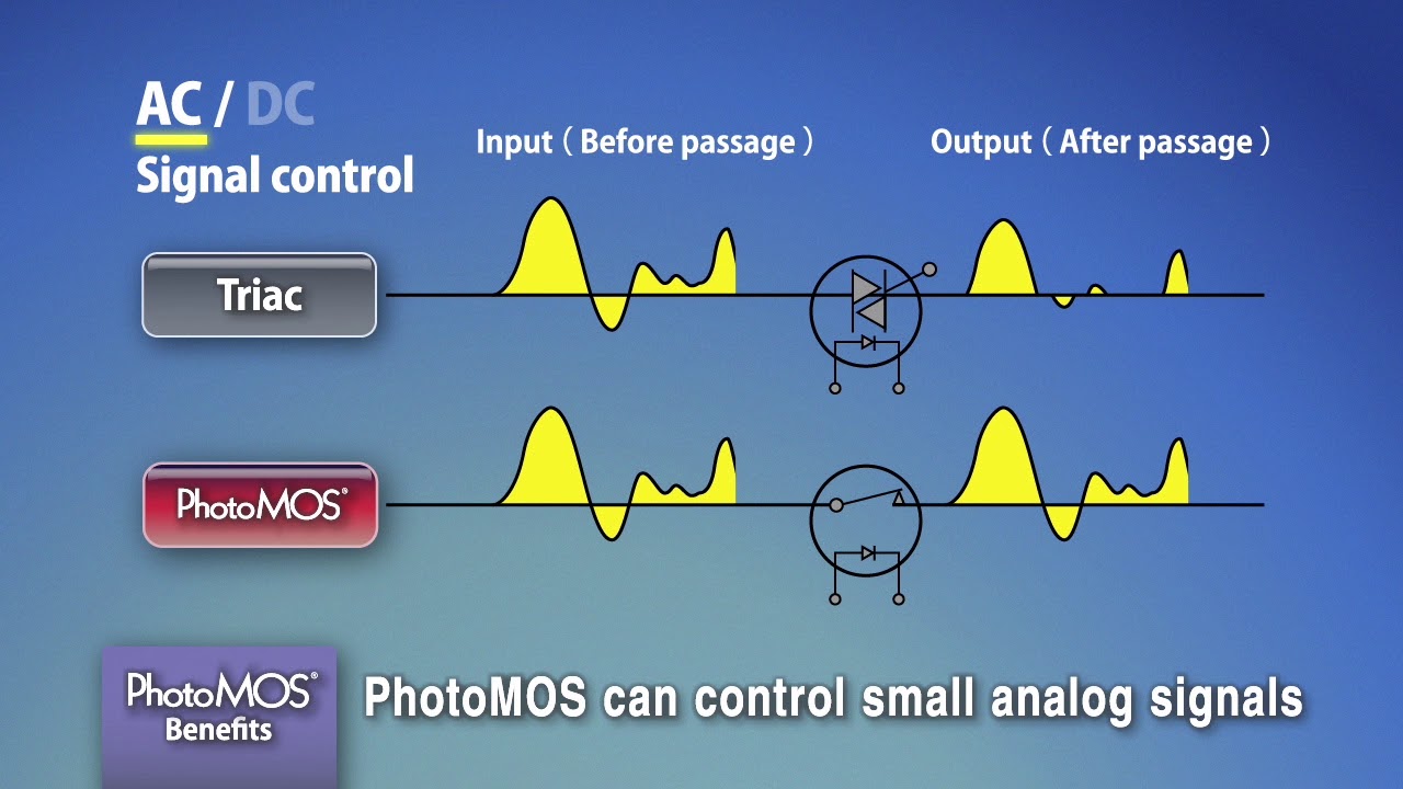
Features and Benefits of PhotoMOS®
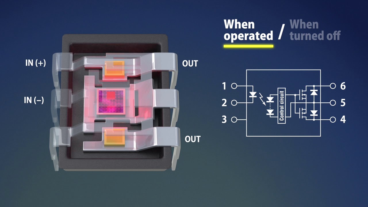
Introduction to PhotoMOS®
New Product Spotlight: PhotoMOS® HE 1 Form A and HE SOP 1 Form A Series Relays
NPI: PhotoMOS® HF 1 Form A Series High Capacity Relays
NPI: Photovoltaic MOSFET PhotoMOS® Relays
New Product Brief: Photovoltaic MOSFET Driver High Power Type
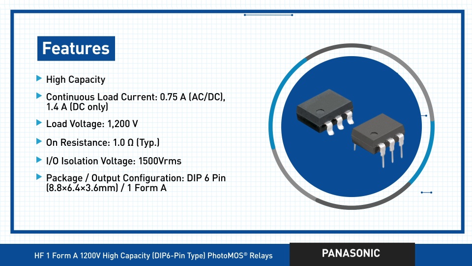
NPI: PhotoMOS HF 1 Form A High Capacity Relays
NPI: PhotoMOS CC TSON 1 Form B
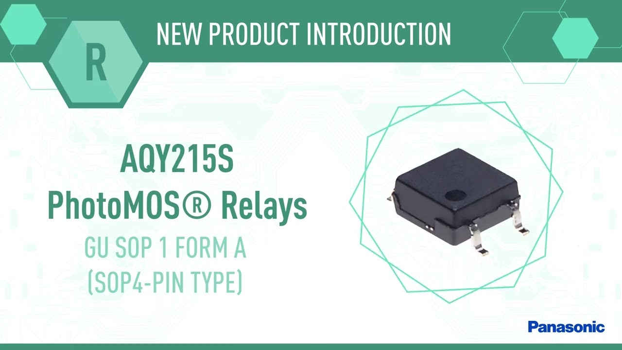
NPI: AQY215S PhotoMOS® Relays
