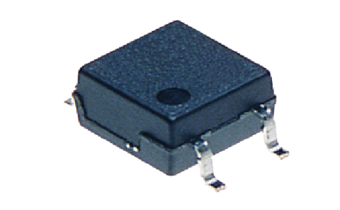
DIP8
AC/DC
60 V
0.5 A
5,000 Vrms
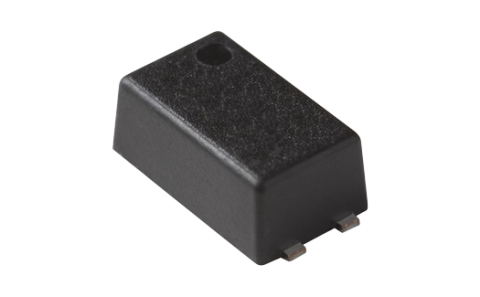
Surface-mount terminal
Tube packing style
GE DIP8 1 Form A & 1 Form B
GE
50 mA
5 V
1 A
75 mW
1.5 A
800 mW
850 mW
-40 to +85℃
-40 to +100℃
1.4 mA (N.C.) (N.O.)
3 mA (N.C.) (N.O.)
0.4 mA (N.C.) (N.O.)
1.3 mA (N.C.) (N.O.)
1.25 V
1.5 V
1 Ω
2.5 Ω
1μA (N.O.), 10μA (N.C.)
Nothing
1.0 ms (N.O.), 3.0 ms (N.C.)
4.0 ms (N.O.), 10.0 ms (N.C.)
0.05 ms (N.O.), 0.2 ms (N.C.)
1.0 ms
0.8 pF
1.5 pF
1,000 M ohm
Min.: 5 mA, Max.: 30 mA
Max.: 48 V
Max.: 0.6 A (1ch), 0.5 A (2ch)
1 Form A 1 Form B
500 mA
125℃
50
500
DIP8
AC/DC
350 V
0.12 A
5,000 Vrms
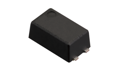
Surface-mount terminal
Tube packing style
GE DIP8 1 Form A & 1 Form B
GE
50 mA
5 V
1 A
75 mW
0.36 A
800 mW
850 mW
-40 to +85℃
-40 to +100℃
1.4 mA (N.C.) (N.O.)
3 mA (N.C.) (N.O.)
0.4 mA (N.C.) (N.O.)
1.3 mA (N.C.) (N.O.)
1.25 V
1.5 V
18 Ω
25 Ω
1μA (N.O.), 10μA (N.C.)
Nothing
0.5 ms (N.O.), 1.0 ms (N.C.)
3.0 ms
0.08 ms (N.O.), 0.3 ms (N.C.)
1.0 ms
0.8 pF
1.5 pF
1,000 M ohm
Min.: 5 mA, Max.: 30 mA
Max.: 280 V
Max.: 0.14 A (1ch), 0.12 A (2ch)
1 Form A 1 Form B
120 mA
125℃
50
500
DIP8
AC/DC
400 V
0.1 A
5,000 Vrms
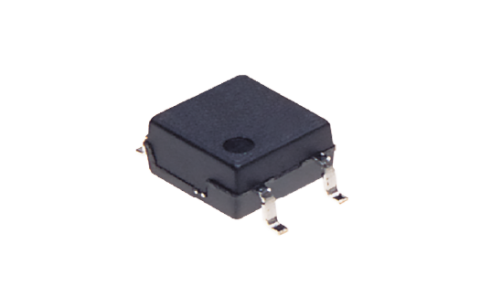
Surface-mount terminal
Tube packing style
GE DIP8 1 Form A & 1 Form B
GE
50 mA
5 V
1 A
75 mW
0.3 A
800 mW
850 mW
-40 to +85℃
-40 to +100℃
1.4 mA (N.C.) (N.O.)
3 mA (N.C.) (N.O.)
0.4 mA (N.C.) (N.O.)
1.3 mA (N.C.) (N.O.)
1.25 V
1.5 V
26 Ω
35 Ω
1μA (N.O.), 10μA (N.C.)
Nothing
0.5 ms (N.O.), 0.8 ms (N.C.)
3.0 ms
0.08 ms (N.O.), 0.2 ms (N.C.)
1.0 ms
0.8 pF
1.5 pF
1,000 M ohm
Min.: 5 mA, Max.: 30 mA
Max.: 320 V
Max.: 0.13 A (1ch), 0.1 A (2ch)
1 Form A 1 Form B
100 mA
125℃
50
500
DIP8
AC/DC
60 V
0.5 A
5,000 Vrms
Surface-mount terminal
Tape and reel packing style (Z)
GE DIP8 1 Form A & 1 Form B
GE
50 mA
5 V
1 A
75 mW
1.5 A
800 mW
850 mW
-40 to +85℃
-40 to +100℃
1.4 mA (N.C.) (N.O.)
3 mA (N.C.) (N.O.)
0.4 mA (N.C.) (N.O.)
1.3 mA (N.C.) (N.O.)
1.25 V
1.5 V
1 Ω
2.5 Ω
1μA (N.O.), 10μA (N.C.)
Nothing
1.0 ms (N.O.), 3.0 ms (N.C.)
4.0 ms (N.O.), 10.0 ms (N.C.)
0.05 ms (N.O.), 0.2 ms (N.C.)
1.0 ms
0.8 pF
1.5 pF
1,000 M ohm
Min.: 5 mA, Max.: 30 mA
Max.: 48 V
Max.: 0.6 A (1ch), 0.5 A (2ch)
1 Form A 1 Form B
500 mA
125℃
1,000
1,000
DIP8
AC/DC
400 V
0.1 A
5,000 Vrms
Surface-mount terminal
Tape and reel packing style (Z)
GE DIP8 1 Form A & 1 Form B
GE
50 mA
5 V
1 A
75 mW
0.3 A
800 mW
850 mW
-40 to +85℃
-40 to +100℃
1.4 mA (N.C.) (N.O.)
3 mA (N.C.) (N.O.)
0.4 mA (N.C.) (N.O.)
1.3 mA (N.C.) (N.O.)
1.25 V
1.5 V
26 Ω
35 Ω
1μA (N.O.), 10μA (N.C.)
Nothing
0.5 ms (N.O.), 0.8 ms (N.C.)
3.0 ms
0.08 ms (N.O.), 0.2 ms (N.C.)
1.0 ms
0.8 pF
1.5 pF
1,000 M ohm
Min.: 5 mA, Max.: 30 mA
Max.: 320 V
Max.: 0.13 A (1ch), 0.1 A (2ch)
1 Form A 1 Form B
100 mA
125℃
1,000
1,000
DIP8
AC/DC
60 V
0.5 A
5,000 Vrms
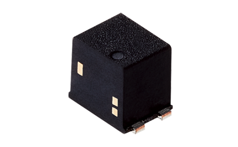
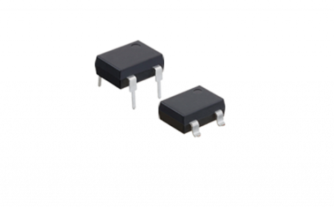
Through hole terminal
Tube packing style
GE DIP8 1 Form A & 1 Form B
GE
50 mA
5 V
1 A
75 mW
1.5 A
800 mW
850 mW
-40 to +85℃
-40 to +100℃
1.4 mA (N.C.) (N.O.)
3 mA (N.C.) (N.O.)
0.4 mA (N.C.) (N.O.)
1.3 mA (N.C.) (N.O.)
1.25 V
1.5 V
1 Ω
2.5 Ω
1μA (N.O.), 10μA (N.C.)
Nothing
1.0 ms (N.O.), 3.0 ms (N.C.)
4.0 ms (N.O.), 10.0 ms (N.C.)
0.05 ms (N.O.), 0.2 ms (N.C.)
1.0 ms
0.8 pF
1.5 pF
1,000 M ohm
Min.: 5 mA, Max.: 30 mA
Max.: 48 V
Max.: 0.6 A (1ch), 0.5 A (2ch)
1 Form A 1 Form B
500 mA
125℃
50
500
DIP8
AC/DC
60 V
0.5 A
5,000 Vrms
Surface-mount terminal
Tape and reel packing style (X)
GE DIP8 1 Form A & 1 Form B
GE
50 mA
5 V
1 A
75 mW
1.5 A
800 mW
850 mW
-40 to +85℃
-40 to +100℃
1.4 mA (N.C.) (N.O.)
3 mA (N.C.) (N.O.)
0.4 mA (N.C.) (N.O.)
1.3 mA (N.C.) (N.O.)
1.25 V
1.5 V
1 Ω
2.5 Ω
1μA (N.O.), 10μA (N.C.)
Nothing
1.0 ms (N.O.), 3.0 ms (N.C.)
4.0 ms (N.O.), 10.0 ms (N.C.)
0.05 ms (N.O.), 0.2 ms (N.C.)
1.0 ms
0.8 pF
1.5 pF
1,000 M ohm
Min.: 5 mA, Max.: 30 mA
Max.: 48 V
Max.: 0.6 A (1ch), 0.5 A (2ch)
1 Form A 1 Form B
500 mA
125℃
1,000
1,000
DIP8
AC/DC
400 V
0.1 A
5,000 Vrms
Through hole terminal
Tube packing style
GE DIP8 1 Form A & 1 Form B
GE
50 mA
5 V
1 A
75 mW
0.3 A
800 mW
850 mW
-40 to +85℃
-40 to +100℃
1.4 mA (N.C.) (N.O.)
3 mA (N.C.) (N.O.)
0.4 mA (N.C.) (N.O.)
1.3 mA (N.C.) (N.O.)
1.25 V
1.5 V
26 Ω
35 Ω
1μA (N.O.), 10μA (N.C.)
Nothing
0.5 ms (N.O.), 0.8 ms (N.C.)
3.0 ms
0.08 ms (N.O.), 0.2 ms (N.C.)
1.0 ms
0.8 pF
1.5 pF
1,000 M ohm
Min.: 5 mA, Max.: 30 mA
Max.: 320 V
Max.: 0.13 A (1ch), 0.1 A (2ch)
1 Form A 1 Form B
100 mA
125℃
50
500
DIP8
AC/DC
400 V
0.1 A
5,000 Vrms
Surface-mount terminal
Tape and reel packing style (X)
GE DIP8 1 Form A & 1 Form B
GE
50 mA
5 V
1 A
75 mW
0.3 A
800 mW
850 mW
-40 to +85℃
-40 to +100℃
1.4 mA (N.C.) (N.O.)
3 mA (N.C.) (N.O.)
0.4 mA (N.C.) (N.O.)
1.3 mA (N.C.) (N.O.)
1.25 V
1.5 V
26 Ω
35 Ω
1μA (N.O.), 10μA (N.C.)
Nothing
0.5 ms (N.O.), 0.8 ms (N.C.)
3.0 ms
0.08 ms (N.O.), 0.2 ms (N.C.)
1.0 ms
0.8 pF
1.5 pF
1,000 M ohm
Min.: 5 mA, Max.: 30 mA
Max.: 320 V
Max.: 0.13 A (1ch), 0.1 A (2ch)
1 Form A 1 Form B
100 mA
125℃
1,000
1,000
DIP8
AC/DC
350 V
0.12 A
5,000 Vrms
Through hole terminal
Tube packing style
GE DIP8 1 Form A & 1 Form B
GE
50 mA
5 V
1 A
75 mW
0.36 A
800 mW
850 mW
-40 to +85℃
-40 to +100℃
1.4 mA (N.C.) (N.O.)
3 mA (N.C.) (N.O.)
0.4 mA (N.C.) (N.O.)
1.3 mA (N.C.) (N.O.)
1.25 V
1.5 V
18 Ω
25 Ω
1μA (N.O.), 10μA (N.C.)
Nothing
0.5 ms (N.O.), 1.0 ms (N.C.)
3.0 ms
0.08 ms (N.O.), 0.3 ms (N.C.)
1.0 ms
0.8 pF
1.5 pF
1,000 M ohm
Min.: 5 mA, Max.: 30 mA
Max.: 280 V
Max.: 0.14 A (1ch), 0.12 A (2ch)
1 Form A 1 Form B
120 mA
125℃
50
500