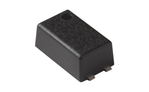
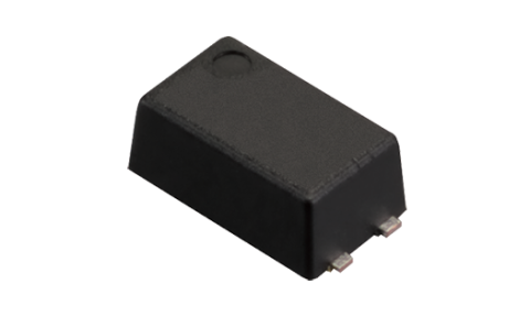
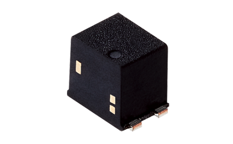
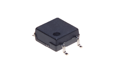
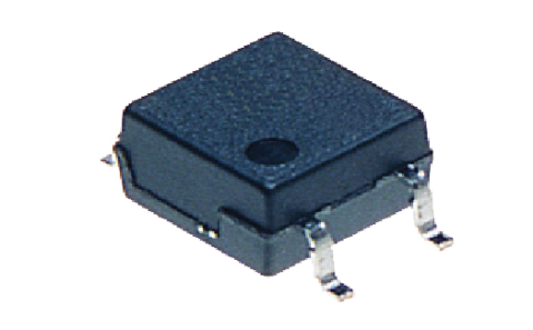
| | SON | AC/DC | Surface-mount terminal | Tape and reel packing style (W) | 40 V | 250 mA | RF SON 1 Form A Low CxR | RF | 1 Form A | 3,500 | 3,500 | 50 mA | 5 V | 1 A | 75 mW | 40 V | 0.25 A | 250 mW | 300 mW | 200 Vrms | -40 to +85℃ | -40 to +100℃ | 125℃ | 0.8 mA | 3.0 mA | 0.1 mA | 0.7 mA | 1.14 V | 1.5 V | 0.8 Ω | 0.8 | 1.25 Ω | 14 pF | 14 | 18 pF | 0.02 nA | 10 nA | Nothing | 0.2 ms | 0.5 ms | 0.04 ms | 0.2 ms | 0.8 pF | 1.5 pF | Min.: 5 mA, Max.: 30 mA | Max.: 15 V | Max.: 0.25 A | 0.75 A | | |
| | SON | AC/DC | Surface-mount terminal | Tape and reel packing style (Y) | 40 V | 250 mA | RF SON 1 Form A Low CxR | RF | 1 Form A | 3,500 | 3,500 | 50 mA | 5 V | 1 A | 75 mW | 40 V | 0.25 A | 250 mW | 300 mW | 200 Vrms | -40 to +85℃ | -40 to +100℃ | 125℃ | 0.8 mA | 3.0 mA | 0.1 mA | 0.7 mA | 1.14 V | 1.5 V | 0.8 Ω | 0.8 | 1.25 Ω | 14 pF | 14 | 18 pF | 0.02 nA | 10 nA | Nothing | 0.2 ms | 0.5 ms | 0.04 ms | 0.2 ms | 0.8 pF | 1.5 pF | Min.: 5 mA, Max.: 30 mA | Max.: 15 V | Max.: 0.25 A | 0.75 A | | |
| | SON | AC/DC | Surface-mount terminal | Tape and reel packing style (Y) | 40 V | 120 mA | RF SON 1 Form A Low CxR | RF | 1 Form A | 3,500 | 3,500 | 50 mA | 5 V | 1 A | 75 mW | 40 V | 0.12 A | 250 mW | 300 mW | 200 Vrms | -40 to +85℃ | -40 to +100℃ | 125℃ | 1.0 mA | 3.0 mA | 0.2 mA | 0.9 mA | 1.14 V | 1.5 V | 9.5 Ω | 9.5 | 12.5 Ω | 1.1 pF | 1.1 | 1.5 pF | 0.01 nA | 10 nA | Nothing | 0.02 ms | 0.2 ms | 0.02 ms | 0.2 ms | 0.8 pF | 1.5 pF | Min.: 5 mA, Max.: 30 mA | Max.: 15 V | Max.: 0.12 A | | | |
| | SON | AC/DC | Surface-mount terminal | Tape and reel packing style (W) | 40 V | 120 mA | RF SON 1 Form A Low CxR | RF | 1 Form A | 3,500 | 3,500 | 50 mA | 5 V | 1 A | 75 mW | 40 V | 0.12 A | 250 mW | 300 mW | 200 Vrms | -40 to +85℃ | -40 to +100℃ | 125℃ | 1.0 mA | 3.0 mA | 0.2 mA | 0.9 mA | 1.14 V | 1.5 V | 9.5 Ω | 9.5 | 12.5 Ω | 1.1 pF | 1.1 | 1.5 pF | 0.01 nA | 10 nA | Nothing | 0.02 ms | 0.2 ms | 0.02 ms | 0.2 ms | 0.8 pF | 1.5 pF | Min.: 5 mA, Max.: 30 mA | Max.: 15 V | Max.: 0.12 A | | | |
| | SON | AC/DC | Surface-mount terminal | Tape and reel packing style (W) | 25 V | 150 mA | RF SON 1 Form A Low CxR | RF | 1 Form A | 3,500 | 3,500 | 50 mA | 5 V | 1 A | 75 mW | 25 V | 0.15 A | 250 mW | 300 mW | 200 Vrms | -40 to +85℃ | -40 to +100℃ | 125℃ | 1.0 mA | 3.0 mA | 0.2 mA | 0.9 mA | 1.14 V | 1.5 V | 5.5 Ω | 5.5 | 7.5 Ω | 1.1 pF | 1.1 | 1.5 pF | 0.01 nA | 10 nA | Nothing | 0.02 ms | 0.2 ms | 0.02 ms | 0.2 ms | 0.8 pF | 1.5 pF | Min.: 5 mA, Max.: 30 mA | Max.: 15 V | Max.: 0.15 A | | | |
| | SON | AC/DC | Surface-mount terminal | Tape and reel packing style (1Y) | 25 V | 150 mA | RF SON 1 Form A Low CxR | RF | 1 Form A | 1,000 | 1,000 | 50 mA | 5 V | 1 A | 75 mW | 25 V | 0.15 A | 250 mW | 300 mW | 200 Vrms | -40 to +85℃ | -40 to +100℃ | 125℃ | 1.0 mA | 3.0 mA | 0.2 mA | 0.9 mA | 1.14 V | 1.5 V | 5.5 Ω | 5.5 | 7.5 Ω | 1.1 pF | 1.1 | 1.5 pF | 0.01 nA | 10 nA | Nothing | 0.02 ms | 0.2 ms | 0.02 ms | 0.2 ms | 0.8 pF | 1.5 pF | Min.: 5 mA, Max.: 30 mA | Max.: 15 V | Max.: 0.15 A | | | |
| | SON | AC/DC | Surface-mount terminal | Tape and reel packing style (1Y) | 40 V | 120 mA | RF SON 1 Form A Low CxR | RF | 1 Form A | 1,000 | 1,000 | 50 mA | 5 V | 1 A | 75 mW | 40 V | 0.12 A | 250 mW | 300 mW | 200 Vrms | -40 to +85℃ | -40 to +100℃ | 125℃ | 1.0 mA | 3.0 mA | 0.2 mA | 0.9 mA | 1.14 V | 1.5 V | 9.5 Ω | 9.5 | 12.5 Ω | 1.1 pF | 1.1 | 1.5 pF | 0.01 nA | 10 nA | Nothing | 0.02 ms | 0.2 ms | 0.02 ms | 0.2 ms | 0.8 pF | 1.5 pF | Min.: 5 mA, Max.: 30 mA | Max.: 15 V | Max.: 0.12 A | | | |
| | SON | AC/DC | Surface-mount terminal | Tape and reel packing style (1Y) | 40 V | 250 mA | RF SON 1 Form A Low CxR | RF | 1 Form A | 1,000 | 1,000 | 50 mA | 5 V | 1 A | 75 mW | 40 V | 0.25 A | 250 mW | 300 mW | 200 Vrms | -40 to +85℃ | -40 to +100℃ | 125℃ | 0.8 mA | 3.0 mA | 0.1 mA | 0.7 mA | 1.14 V | 1.5 V | 0.8 Ω | 0.8 | 1.25 Ω | 14 pF | 14 | 18 pF | 0.02 nA | 10 nA | Nothing | 0.2 ms | 0.5 ms | 0.04 ms | 0.2 ms | 0.8 pF | 1.5 pF | Min.: 5 mA, Max.: 30 mA | Max.: 15 V | Max.: 0.25 A | 0.75 A | | |
| | SON | AC/DC | Surface-mount terminal | Tape and reel packing style (Y) | 25 V | 150 mA | RF SON 1 Form A Low CxR | RF | 1 Form A | 3,500 | 3,500 | 50 mA | 5 V | 1 A | 75 mW | 25 V | 0.15 A | 250 mW | 300 mW | 200 Vrms | -40 to +85℃ | -40 to +100℃ | 125℃ | 1.0 mA | 3.0 mA | 0.2 mA | 0.9 mA | 1.14 V | 1.5 V | 5.5 Ω | 5.5 | 7.5 Ω | 1.1 pF | 1.1 | 1.5 pF | 0.01 nA | 10 nA | Nothing | 0.02 ms | 0.2 ms | 0.02 ms | 0.2 ms | 0.8 pF | 1.5 pF | Min.: 5 mA, Max.: 30 mA | Max.: 15 V | Max.: 0.15 A | | | |