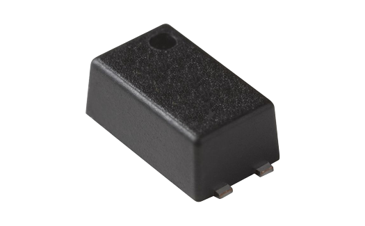
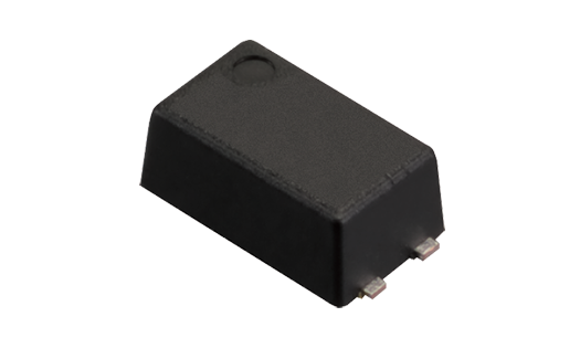
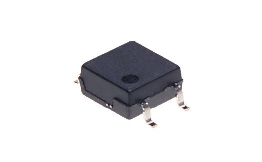
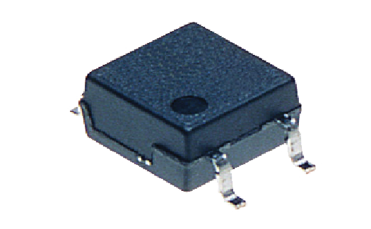
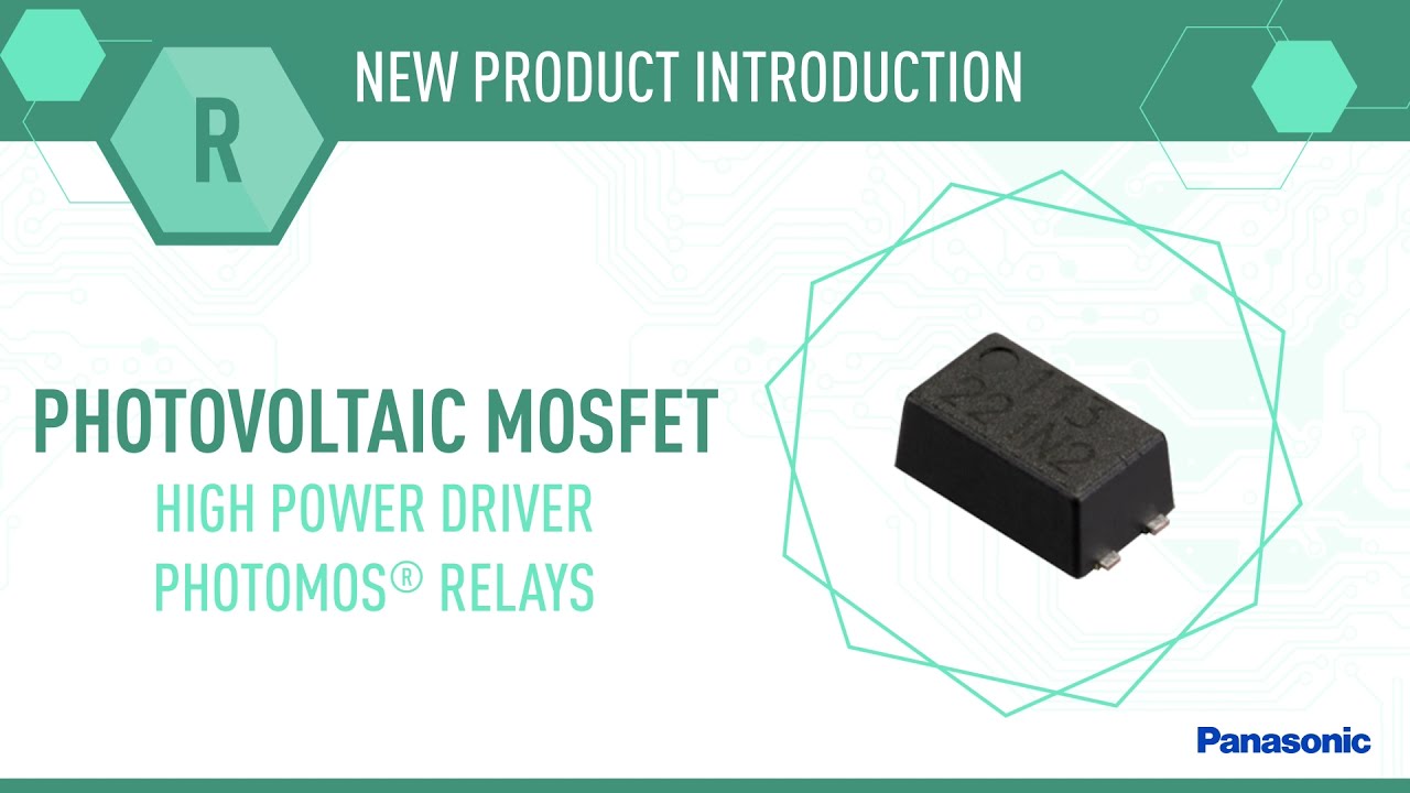
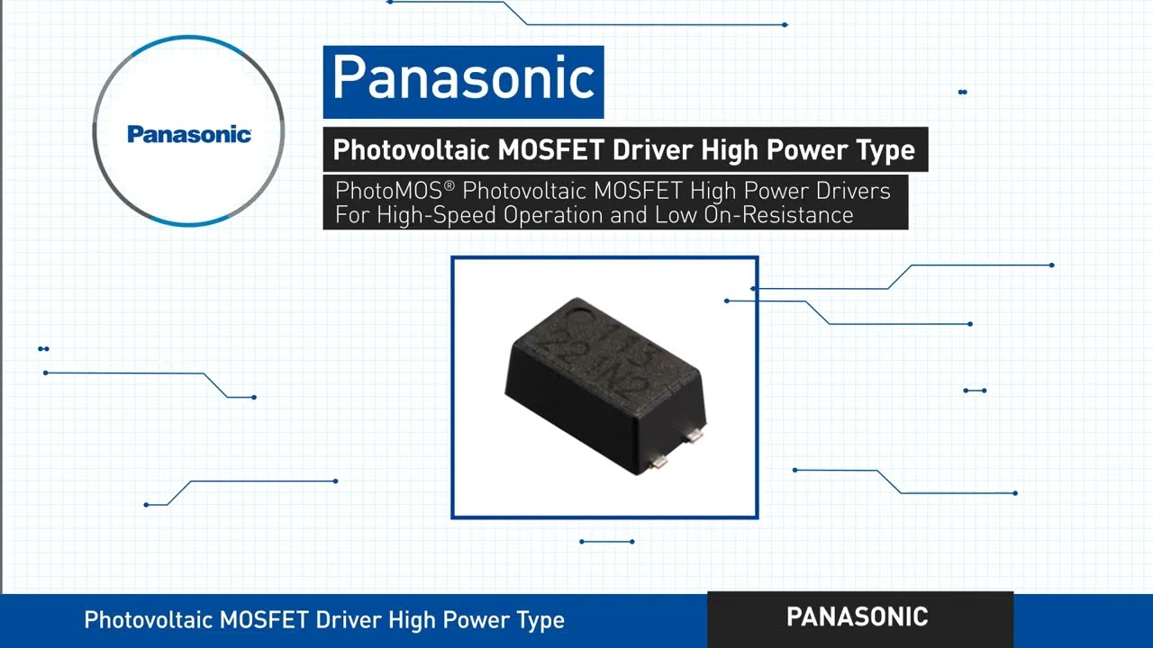
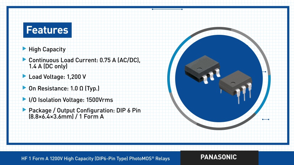
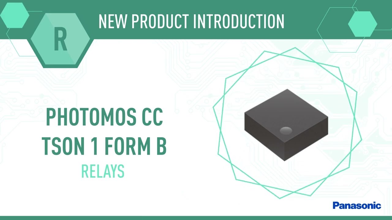
The PhotoMOS® CC Series is a revolution in size and performance. The internal switching mechanism contains an oscillation circuit as well as a built-in Capacitor-Coupled Isolation driver IC. This differs from traditional PhotoMOS products which use an optically coupled isolation. By replacing the LED circuit, the package size can be substantially decreased, while also lowering power consumption.
 
Features:

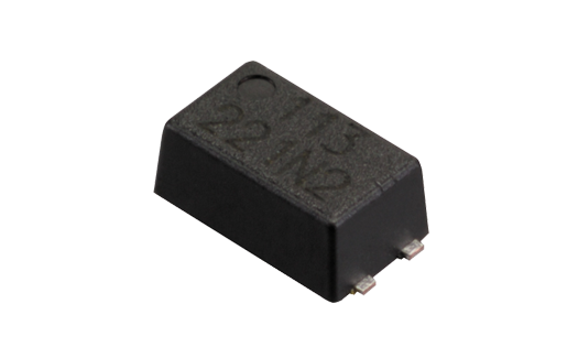
  • Sub-Miniature TSON Package (0.8 x 1.95 x 1.8mm)
  • Low Current Consumption of 0.2A Max.
  • High Temp Performance, Guaranteed to 105C
  • Voltage-Driven Input Circuit
  • RoHS/REACH Compliant

Benefits:

  • 46% Less Board Space Than SON
  • Contributes to Energy Savings
  • Robust Performance in Industrial Applications
  • Faster Switching Speeds
  • Environmentally Friendly

PhotoMOS CC TSON 1 Form A CxR

Part number list

Results 15
Models table for series PhotoMOS CC TSON 1 Form A CxR
Part No.DatasheetPackageVoltage TypeLoad Voltage [ VL ] (VL)Continuous Load Current (IL)I/O Isolation Voltage (Viso)Contact ArrangementPacking QuantityProduct NameTypeInput Reverse Voltage (VRIN)Input Voltage (VIN)Power Dissipation (Pin)Peak Load Current (Ipeak)Power Dissipation (Pout)Total Power Dissipation (Pt)Ambient Temperature: Operating (Topr)Ambient Temperature: Storage (Tstg)Operate Voltage (Typical) (VFon)Operate Voltage (Maximum) (VFon)Turn Off Voltage (Minimum) (VFoff)Turn Off Voltage (Typical) (VFoff)Input Current (Typical) (IIN)Input Current (Maximum) (IIN)On Resistance (Typical) (Ron)On Resistance (Maximum) (Ron)Output Capacitance (Typical) (Cout)Output Capacitance (Maximum) (Cout)Off State Leakage Current (Maximum) (ILeak)Over Current ProtectionTurn On Time (Typical) Turn On Time (Maximum) Turn Off Time (Typical)Turn Off Time (Maximum)I/O Capacitance (Typical) (Ciso)I/O Capacitance (Maximum) (Ciso)Input Voltage (VIN)Load Voltage (VL)Continuous Load Current (IL)Terminal TypeExternal DimensionsRecommended Mounting Pad (Top View) I/O Capacitance (Typical) (Ciso)Load currentLoad Voltage [ VL ] Packing quantity
1-reel (pcs.)
Packing quantity
Outer carton (pcs.)
Off State Leakage Current (Maximum) (ILeak)Total Power Dissipation (Pt)Ambient Temperature: Operating (Topr)Ambient Temperature: Storage (Tstg)Operate Voltage (Typical) (VFon)
TSON
AC/DC
40 V
0.1 A
200 Vrms
1 Form A
Tape and reel packing style (Z)
CC TSON Low CxR
CC
0.2 V
5.5 V
1.2 mW
0.3 A
250 mW
250 mW
-40 to +105°C
-40 to +125°C
2.2 V
2.5 V
0.5 V
1.5 V
0.09 mA
0.2 mA
10.5 ohm
15 ohm
1.2 pF
2 pF
10nA
Nothing
0.01 ms
0.1 ms
0.02 ms
0.2 ms
3 pF
Min.: 3 V, Max.: 5 V
Max.: 15 V
Max.: 0.1 A
Surface-mount terminal
1.2 pF
0.1 A
40 V
3,500
3,500
10nA
TSON
AC/DC
30 V
0.75 A
200 Vrms
1 Form A
Tape and reel packing style (X)
CC TSON Low CxR
CC
0.2 V
5.5 V
1.2 mW
1.5 A
250 mW
250 mW
-40 to +105°C
-40 to +125°C
1.7 V
2.5 V
0.5 V
1.5 V
0.09 mA
0.2 mA
0.2 ohm
0.4 ohm
40 pF
100 pF
10nA
Nothing
0.12 ms
0.5 ms
0.1 ms
0.5 ms
3 pF
Min.: 3 V, Max.: 5 V
Max.: 15 V
Max.: 0.75 A
Surface-mount terminal
1.2 pF
0.75 A
30 V
3,500
3,500
TSON
AC/DC
30 V
0.75 A
200 Vrms
1 Form A
Tape and reel packing style (Z)
CC TSON Low CxR
CC
0.2 V
5.5 V
1.2 mW
1.5 A
250 mW
250 mW
-40 to +105°C
-40 to +125°C
1.7 V
2.5 V
0.5 V
1.5 V
0.09 mA
0.2 mA
0.2 ohm
0.4 ohm
40 pF
100 pF
10nA
Nothing
0.12 ms
0.5 ms
0.1 ms
0.5 ms
3 pF
Min.: 3 V, Max.: 5 V
Max.: 15 V
Max.: 0.75 A
Surface-mount terminal
1.2 pF
0.75 A
30 V
3,500
3,500
TSON
AC/DC
40 V
0.3 A
200 Vrms
1 Form A
Tape and reel packing style (X)
CC TSON Low CxR
CC
0.2 V
5.5 V
1.2 mW
0.75 A
250 mW
250 mW
-40 to +105°C
-40 to +125°C
1.8 V
2.5 V
0.5 V
1.4 V
0.09 mA
0.2 mA
0.8 ohm
1.5 ohm
14.5 pF
18 pF
10nA
Nothing
0.06 ms
0.5 ms
0.06 ms
0.5 ms
3 pF
Min.: 3 V, Max.: 5 V
Max.: 15 V
Max.: 0.3 A
Surface-mount terminal
1.2 pF
0.3 A
40 V
3,500
3,500
TSON
AC/DC
30 V
0.75 A
200 Vrms
1 Form A
Tape and reel packing style (1X)
CC TSON Low CxR
CC
0.2 V
5.5 V
1.2 mW
1.5 A
250 mW
250 mW
-40 to +105°C
-40 to +125°C
1.7 V
2.5 V
0.5 V
1.5 V
0.09 mA
0.2 mA
0.2 ohm
0.4 ohm
40 pF
100 pF
10nA
Nothing
0.12 ms
0.5 ms
0.1 ms
0.5 ms
3 pF
Min.: 3 V, Max.: 5 V
Max.: 15 V
Max.: 0.75 A
Surface-mount terminal
1.2 pF
0.75 A
30 V
1,000
1,000
TSON
AC/DC
60 V
0.3 A
200 Vrms
1 Form A
Tape and reel packing style (Z)
CC TSON Low CxR
CC
0.2 V
5.5 V
1.2 mW
0.9 A
250 mW
250 mW
-40 to +105°C
-40 to +125°C
1.7 V
2.5 V
0.5 V
1.4 V
0.09 mA
0.2 mA
0.9 ohm
1.5 ohm
27 pF
40 pF
10nA
Nothing
0.08 ms
0.5 ms
0.1 ms
0.5 ms
3 pF
Min.: 3 V, Max.: 5 V
Max.: 30 V
Max.: 0.3 A
Surface-mount terminal
1.2 pF
0.3 A
60 V
3,500
3,500
TSON
AC/DC
60 V
0.3 A
200 Vrms
1 Form A
Tape and reel packing style (1X)
CC TSON Low CxR
CC
0.2 V
5.5 V
1.2 mW
0.9 A
250 mW
250 mW
-40 to +105°C
-40 to +125°C
1.7 V
2.5 V
0.5 V
1.4 V
0.09 mA
0.2 mA
0.9 ohm
1.5 ohm
27 pF
40 pF
10nA
Nothing
0.08 ms
0.5 ms
0.1 ms
0.5 ms
3 pF
Min.: 3 V, Max.: 5 V
Max.: 30 V
Max.: 0.3 A
Surface-mount terminal
1.2 pF
0.3 A
60 V
1,000
1,000
TSON
AC/DC
40 V
0.3 A
200 Vrms
1 Form A
Tape and reel packing style (1X)
CC TSON Low CxR
CC
0.2 V
5.5 V
1.2 mW
0.75 A
250 mW
250 mW
-40 to +105°C
-40 to +125°C
1.8 V
2.5 V
0.5 V
1.4 V
0.09 mA
0.2 mA
0.8 ohm
1.5 ohm
14.5 pF
18 pF
10nA
Nothing
0.06 ms
0.5 ms
0.06 ms
0.5 ms
3 pF
Min.: 3 V, Max.: 5 V
Max.: 15 V
Max.: 0.3 A
Surface-mount terminal
1.2 pF
0.3 A
40 V
1,000
1,000
TSON
AC/DC
40 V
0.3 A
200 Vrms
1 Form A
Tape and reel packing style (Z)
CC TSON Low CxR
CC
0.2 V
5.5 V
1.2 mW
0.75 A
250 mW
250 mW
-40 to +105°C
-40 to +125°C
1.8 V
2.5 V
0.5 V
1.4 V
0.09 mA
0.2 mA
0.8 ohm
1.5 ohm
14.5 pF
18 pF
10nA
Nothing
0.06 ms
0.5 ms
0.06 ms
0.5 ms
1.2 pF
3 pF
Min.: 3 V, Max.: 5 V
Max.: 15 V
Max.: 0.3 A
Surface-mount terminal
1.2 pF
0.3 A
40 V
3,500
3,500
250 mW
-40 to +105°C -40 to +221°F
-40 to +125°C -40 to +257°F
1.8 V
TSON
AC/DC
60 V
0.3 A
200 Vrms
1 Form A
Tape and reel packing style (X)
CC TSON Low CxR
CC
0.2 V
5.5 V
1.2 mW
0.9 A
250 mW
250 mW
-40 to +105°C
-40 to +125°C
1.7 V
2.5 V
0.5 V
1.4 V
0.09 mA
0.2 mA
0.9 ohm
1.5 ohm
27 pF
40 pF
10nA
Nothing
0.08 ms
0.5 ms
0.1 ms
0.5 ms
3 pF
Min.: 3 V, Max.: 5 V
Max.: 30 V
Max.: 0.3 A
Surface-mount terminal
1.2 pF
0.3 A
60 V
3,500
3,500
Latest Videos

Playlist

Thumbnail for Features and Benefits of PhotoMOS®

Features and Benefits of PhotoMOS®

Thumbnail for Introduction to PhotoMOS®

Introduction to PhotoMOS®

Thumbnail for New Product Spotlight: PhotoMOS® HE 1 Form A and HE SOP 1 Form A Series Relays

New Product Spotlight: PhotoMOS® HE 1 Form A and HE SOP 1 Form A Series Relays

Thumbnail for NPI: PhotoMOS® HF 1 Form A Series High Capacity Relays

NPI: PhotoMOS® HF 1 Form A Series High Capacity Relays

Thumbnail for NPI: Photovoltaic MOSFET PhotoMOS® Relays

NPI: Photovoltaic MOSFET PhotoMOS® Relays

Thumbnail for New Product Brief: Photovoltaic MOSFET Driver High Power Type

New Product Brief: Photovoltaic MOSFET Driver High Power Type

Thumbnail for NPI: PhotoMOS HF 1 Form A High Capacity Relays

NPI: PhotoMOS HF 1 Form A High Capacity Relays

Thumbnail for NPI: PhotoMOS CC TSON 1 Form B

NPI: PhotoMOS CC TSON 1 Form B

Thumbnail for NPI: AQY215S PhotoMOS® Relays

NPI: AQY215S PhotoMOS® Relays

Thumbnail for New Product Introduction: PhotoMOS® GU SOP 1 Form A High-Capacity Semiconductor Relay

New Product Introduction: PhotoMOS® GU SOP 1 Form A High-Capacity Semiconductor Relay