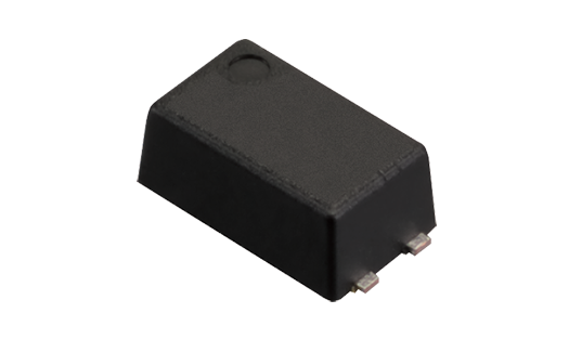
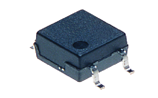
PhotoMOS CC TSON 1 Form B
The Panasonic PhotoMOS® CC Semiconductor Relay offers a super small TSON package, an oscillation circuit, and a built-in capacitor coupled isolation driver IC. These PhotoMOS CC Relays are the latest version of this technology, which now is available as a 1 Form B, customarily closed, contact arrangement. The PhotoMOS CC differs from traditional PhotoMOS products, which use an optically coupled isolation and the current driving method.
Removing the LED from the Relay allows the PhotoMOS CC 1 Form B Type to offer four significant benefits:
- Smaller package size of 0.8 x 1.95 x 1.8 mm, which is the equivalent of 46% less mounting area than Panasonic’s previous SON type package
- Low power consumption with an input current of only 0.2mA maximum
- High operating temperature of 105°C compared to previous 85°C options
- Driven by Voltage instead of Current on the input side
Features / Benefits of the PhotoMOS CC 1 Form B Relay
- Ultra-Miniature TSON Package for Space Savings and Density Mounting
- Low Current Consumption of 0.04 mA Typ. Input Current for Energy Savings and Increased Drivability
- High Temperature Performance at 105°C Max.
- Voltage Driving Type: 3 V to 5 V
- Closed Contact Arrangement
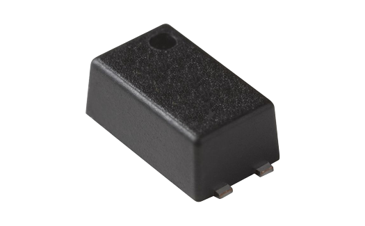
PhotoMOS CC TSON 1 Form B
Part number list
Results 2
Resources
Filter by:
Showing 1 to 10 of 10 results
Results10
What's New
Stay up to date

Latest Videos
Playlist
Features and Benefits of PhotoMOS®
Introduction to PhotoMOS®
New Product Spotlight: PhotoMOS® HE 1 Form A and HE SOP 1 Form A Series Relays
NPI: PhotoMOS® HF 1 Form A Series High Capacity Relays
NPI: Photovoltaic MOSFET PhotoMOS® Relays
New Product Brief: Photovoltaic MOSFET Driver High Power Type
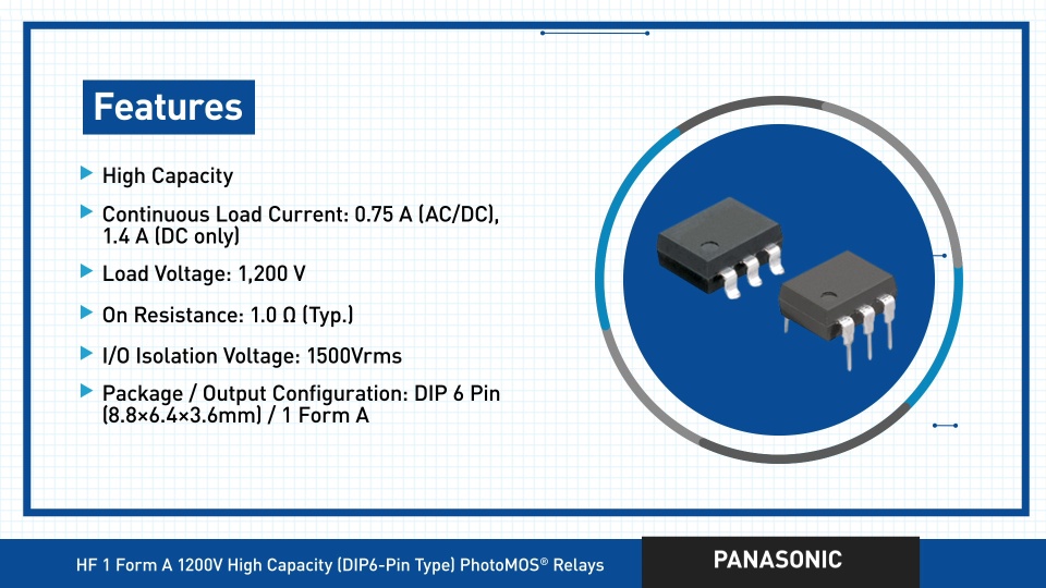
NPI: PhotoMOS HF 1 Form A High Capacity Relays
NPI: PhotoMOS CC TSON 1 Form B
NPI: AQY215S PhotoMOS® Relays