Specifications
| Item | Performance characteristics |
|---|---|
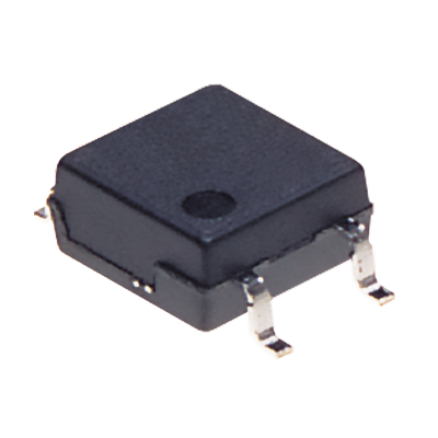
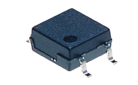
| Package | SOP8 |
| Voltage Type | AC/DC |
| Load Voltage [ V<sub>L</sub> ] (V<sub>L</sub>) | 60 V |
| Continuous Load Current (I<sub>L</sub>) | 0.45 A |
| I/O Isolation Voltage (V<sub>iso</sub>) | 1,500 Vrms |
| Packing Quantity | Tape and reel packing style (Z) |
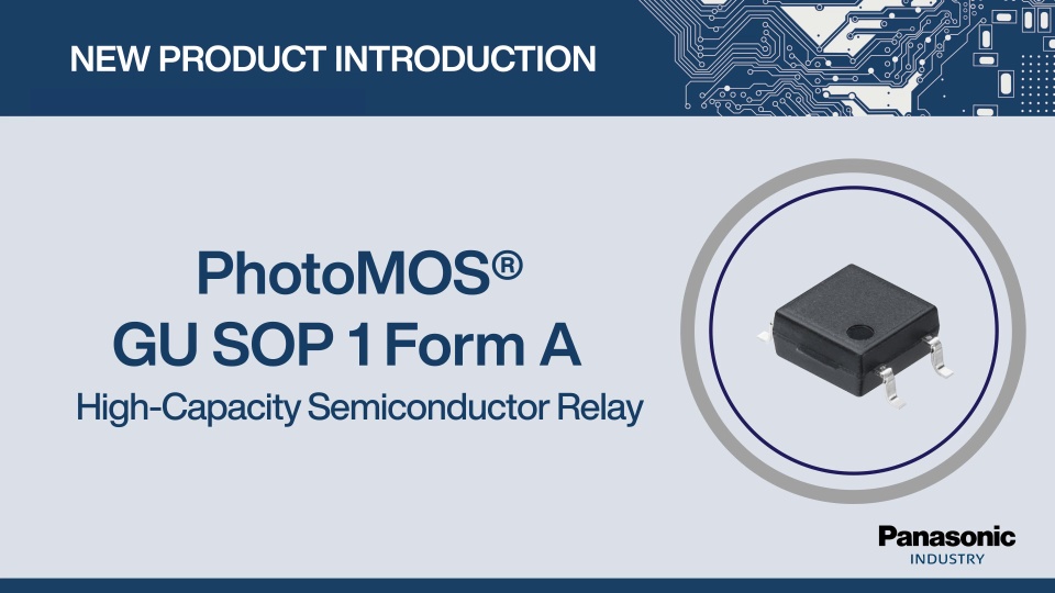
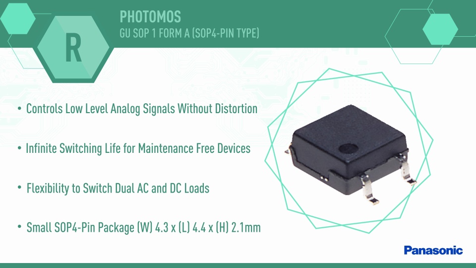
| Product Name | GU SOP 1 Form A & 1 Form B |
| Type | GU |
| LED Forward Current (I<sub>F</sub>) | 50 mA |
| LED Reverse Voltage (V<sub>R</sub>) | 5 V |
| Peak Forward Current (I<sub>FP</sub>) | 1 A |
| Power Dissipation (P<sub>in</sub>) | 75 mW |
| Peak Load Current (I<sub>peak</sub>) | 1.5 A |
| Power Dissipation (P<sub>out</sub>) | 600 mW |
| Total Power Dissipation (P<sub>t</sub>) | 650 mW |
| Ambient Temperature: Operating (T<sub>opr</sub>) | -40 to +85°C |
| Ambient Temperature: Storage (T<sub>stg</sub>) | -40 to +100°C |
| LED Operate Current (Typical) | 0.9 mA |
| LED Operate Current (Maximum) | 3 mA |
| LED Turn Off Current (Minimum) | 0.4 mA |
| LED Turn Off Current (Typical) | 0.8 mA |
| LED Dropout Voltage (Typical) (V<sub>F</sub>) | 1.25 V |
| LED Dropout Voltage (Maximum) (V<sub>F</sub>) | 1.5 V |
| On Resistance (Typical) (R<sub>on</sub>) | 1 ohm |
| On Resistance (Maximum) (R<sub>on</sub>) | 2.5 ohm |
| Off State Leakage Current (Maximum) (I<sub>Leak</sub>) | 1μA |
| Over Current Protection | Nothing |
| Turn On Time (Typical) | 0.65 ms (N.O.), 0.9 ms (N.C.) |
| Turn On Time (Maximum) | 3.0 ms |
| Turn Off Time (Typical) | 0.08 ms (N.O.), 0.2ms (N.C.) |
| Turn Off Time (Maximum) | 1.0 ms |
| I/O Capacitance (Typical) (C<sub>iso</sub>) | 0.8 pF |
| I/O Capacitance (Maximum) (C<sub>iso</sub>) | 1.5 pF |
| Initial I/O Isolation Resistance (Minimum) (R<sub>iso</sub>) | 1,000 M ohm |
| LED Current (I<sub>F</sub>) | Min.: 5 mA, Max.: 30 mA |
| Load Voltage (V<sub>L</sub>) | Max.: 48 V |
| Continuous Load Current (I<sub>L</sub>) | Max.: 0.55 A (1ch), 0.45 A (2ch) |
| Terminal Type | Surface-mount terminal |
| Contact Arrangement | 1 Form A 1 Form B |
| External Dimensions |  |
| Recommended Mounting Pad (Top View) |  |
| Load current | 450 mA |
| Junction temperature (T<sub>j</sub>) | 125°C |
| Packing quantity<br>Outer carton (pcs.) | 1,000 |
| Packing quantity<br>1-reel (pcs.) | 1,000 |
Stock check
AQW612SZ
What's New
Stay up to date


Latest Videos
Playlist
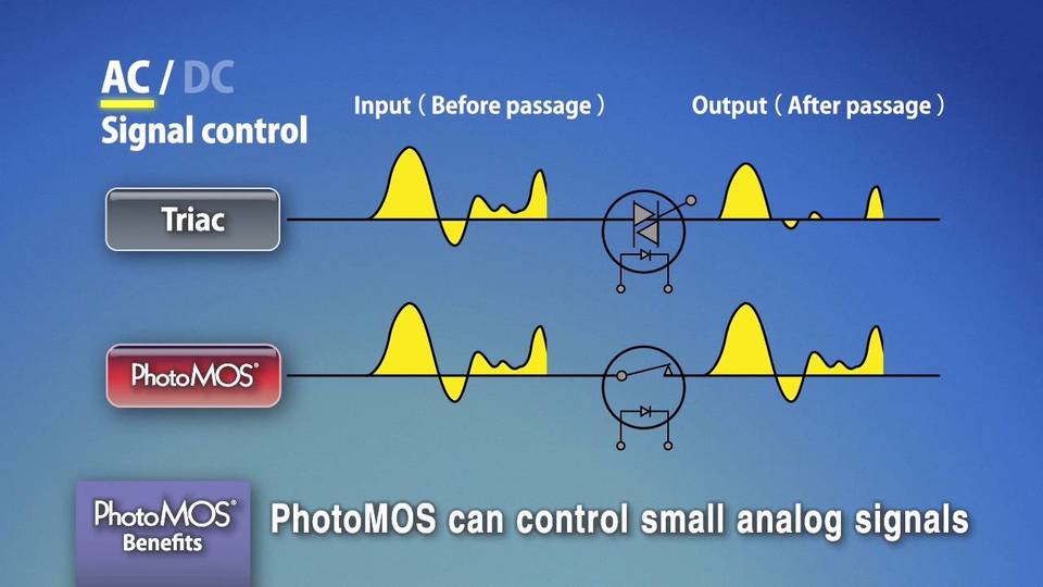
Features and Benefits of PhotoMOS®
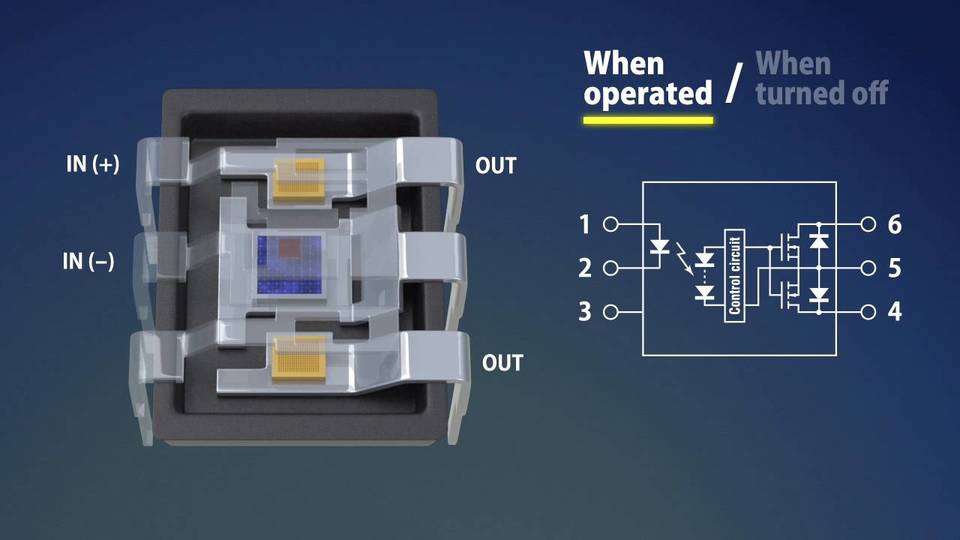
Introduction to PhotoMOS®
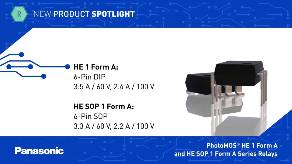
New Product Spotlight: PhotoMOS® HE 1 Form A and HE SOP 1 Form A Series Relays
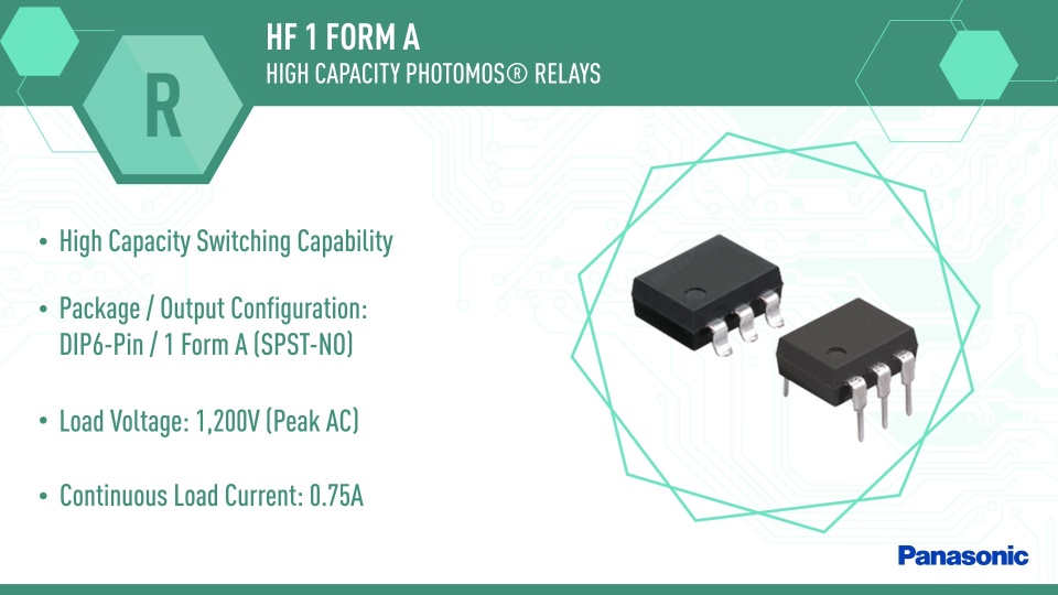
NPI: PhotoMOS® HF 1 Form A Series High Capacity Relays

NPI: Photovoltaic MOSFET PhotoMOS® Relays
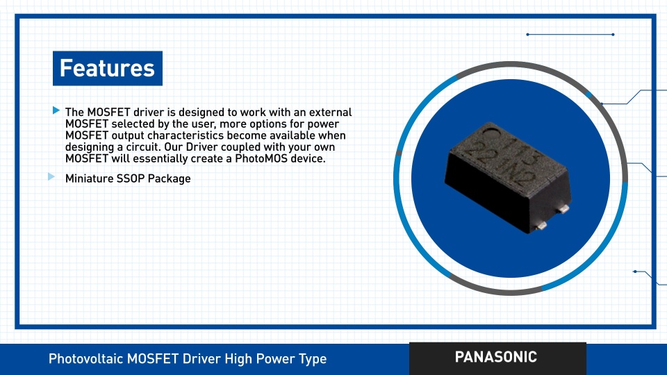
New Product Brief: Photovoltaic MOSFET Driver High Power Type
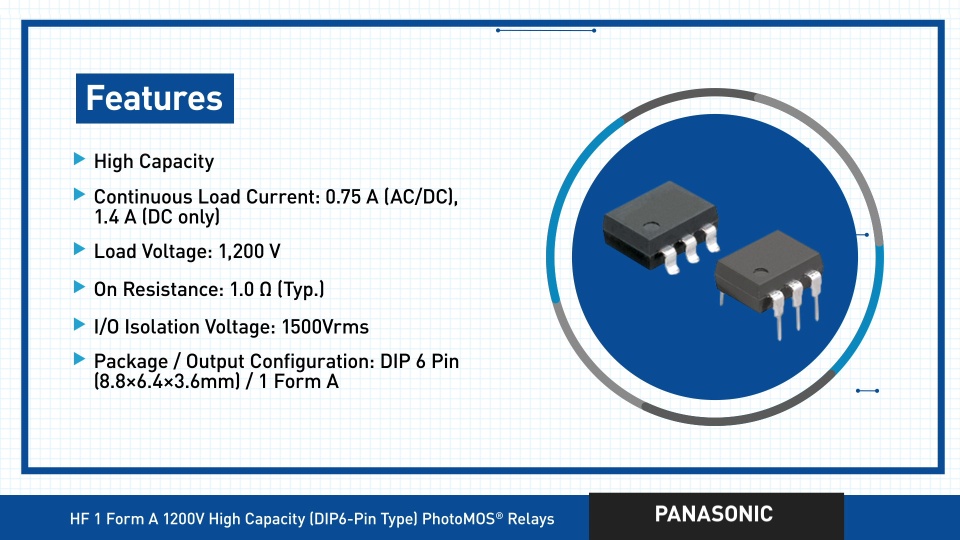
NPI: PhotoMOS HF 1 Form A High Capacity Relays
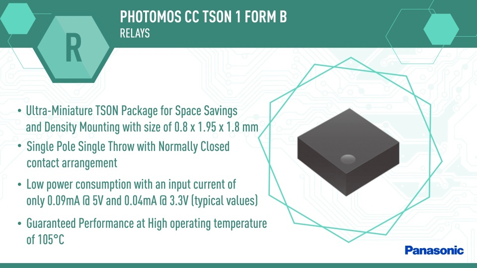
NPI: PhotoMOS CC TSON 1 Form B
NPI: AQY215S PhotoMOS® Relays